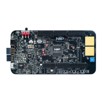
S32K312EVB-Q172 | S32K312EVBQ172ND - Hardware User Manual
S32K312EVB-Q172
S32K312EVBQ172ND
HWUM
All Information provided in this document is subject to legal disclaimers
© NXP B.V. 2020. All rights reserved
Table 15. Default Jumper Configuration
FS26_VLDO1 [+5.0V] is routed to P5V0 domain
FS26_VLDO2 [+3.3V] is routed to P3V3 domain
Flash Mode – configuration in the FS26
P5V0 (+5.0V from the FS26) is selected for the VDD_HV_A_MCU reference.
VDD_HV_A is routed to VDD_HV_A_MCU reference. A jumper on this position disables the shunt
resistors R57 and R58 are disabled for current measurement proposals.
VDD_HV_B is routed to VDD_HV_B_PERH
VDD_HV_A is routed to VDD_HV_A_PERH
 Loading...


