11
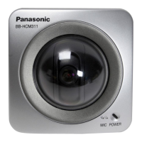
BB-HCM511A/BB-HCM531A
4.2. Camera Block
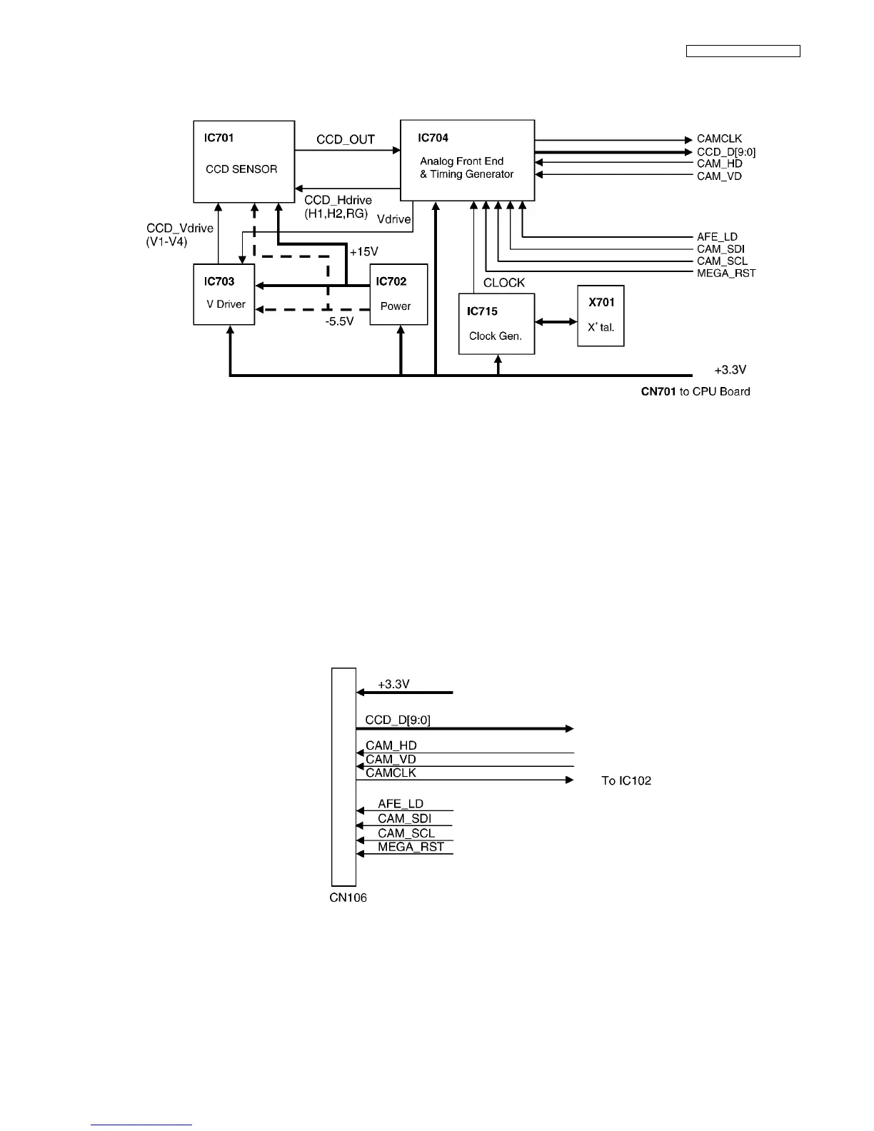
[Camera (CCD) Board]
• C701 is a CCD image sensor module with approx. 320 thousand pixels, and outputs the image signal (CCD_OUT) in VGA size
(640×480).
IC704 outputs Pixel clock (CAMCLK) and CCD_H drive signal based on the timing of synchronized signal (CAM_HD, CAM_VD)
from CPU Board after receiving CLOCK signal from IC715.
• IC704 rejects the noise from CCD_OUT signal and compensates the gain, and then outputs 10-bit data (CCD_D[9:0]).
• The clock signal (CLOCK) of IC704 is 24.5454MHz, which is generated in IC 715 based on the timing of crystal (X701).
• IC704 is controlled by CPU using the serial signal (AFE_LD, CAM_SDI, CAM_SCL).
• The hard reset (MEGA_RST) of IC704 is controlled by GPIO of IC102 in CPU unit.
• IC703 receives the Vdrive timing signal (Vdrive: CH1, CH2, XV1-XV4) from IC704, and IC701 (CCD) outputs Vdrive signal
(CCD_Vdrive :V1-V4).
• +3.3V, -5.5V and 15V are required for the power supply of Camera Unit. +3.3V is input from CPU unit. +15V and -5.5V are gen-
erated from the input (+3.3V) in IC702, and are led to IC701 and IC703.
• The above-mentioned signals and power supplies are connected to CPU Board through CN701.
[CPU Board]
• The image data (CCD_D[9:0]) input from CCD Board to CPU Board and the pixel clock (CAMCLK) are led to CPU (IC102)
through CN106.
• IC102 of CPU Board outputs the synchronized signal (CAM_HD and CAM_VD) and serial signal for AFE control (AFE_LD,
CAM_SDI, CAM_SCL) through CN106.