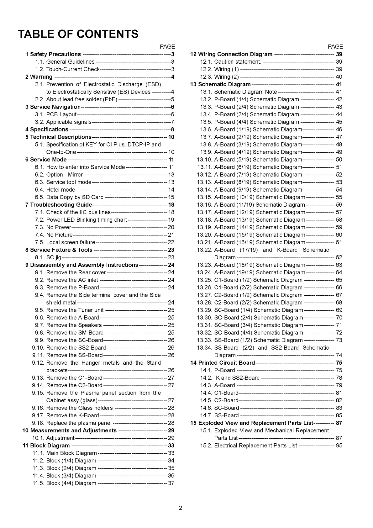
TABLE OF CONTENTS
1 Safety Precautions
----------
1.1. General Guidelines —
1.2. Touch-Current Check-
2 Warning---------------------------
PAGE
------
3
------
3
------
3
------
4
2.1. Prevention of Electrostatic Discharge (ESD)
to Electrostatically Sensitive (ES) Devices
----------
4
2.2. About lead free solder (PbF)-----------------------------5
3 Service Navigation
---------------------------------------------------6
3.1. PCB Layout----------------------------------------------------- 6
3.2. Applicable signals---------------------------------------------7
4 Specifications--------------------------------------------------------- 8
105 Technical Descriptions
-----------------------------------
5.1. Specification of KEY for CI Plus, DTCP-IP and
One-to-One
----------------------------------------------------10
6 Service Mode----------------------------------------------------------11
6.1. How to enter into Service Mode-------------------------11
6.2. Option - Mirror-------------------------------------------------13
6.3. Service tool mode--------------------------------------------13
6.4. Hotel mode----------------------------------------------------- 14
6.5. Data Copy by SD Card------------------------------------15
7 Troubleshooting Guide
-------------------------------------------
18
7.1. Check of the IIC bus lines---------------------------------18
7.2. Power LED Blinking timing chart
-----------------------
19
7.3. No Power-------------------------------------------------------20
7.4. No Picture
------------------------------------------------------
21
7.5. Local screen failure
-----------------------------------------
22
8 Service Fixture & Tools
------------------------------------------
23
8.1. SC jig
------------------------------------------------------------ 23
9 Disassembly and Assembly Instructions-----------------24
9.1. Remove the Rear cover----------------------------------24
9.2. Remove the AC inlet--------------------------------------24
9.3. Remove the P-Board-------------------------------------- 24
9.4. Remove the Side terminal cover and the Side
shield metal----------------------------------------------------24
9.5. Remove the Tuner unit-----------------------------------25
9.6. Remove the A-Board--------------------------------------25
9.7. Remove the Speakers------------------------------------25
9.8. Remove the SM-Board-----------------------------------25
9.9. Remove the SC-Board------------------------------------26
9.10. Remove the SS2-Board----------------------------------26
9.11. Remove the SS-Board------------------------------------26
9.12. Remove the Hanger metals and the Stand
brackets--------------------------------------------------------- 26
9.13. Remove the C1-Board------------------------------------27
9.14. Remove the C2-Board------------------------------------27
9.15. Remove the Plasma panel section from the
Cabinet assy (glass)----------------------------------------27
9.16. Remove the Glass holders
-----------------------------
28
9.17. Remove the K-Board
--------------------------------------
28
9.18. Replace the plasma panel-------------------------------28
10 Measurements and Adjustments
----------------------------
29
10.1. Adjustment-----------------------------------------------------29
11 Block Diagram
------------------------------------------------------
33
11.1. Main Block Diagram
---------------------------------------
33
11.2. Block (1/4) Diagram
---------------------------------------34
11.3. Block (2/4) Diagram---------------------------------------35
11.4. Block (3/4) Diagram---------------------------------------36
11.5. Block (4/4) Diagram---------------------------------------37
12 Wiring Connection Diagram
12.1. Caution statement.
------
12.2. Wiring (1)
-------------------
12.3. Wiring (2) -------------------
13 Schematic Diagram
------------
PAGE
----
39
----
39
----
39
----
40
----
41
----
41
----
42
----
43
----
44
----
45
----
46
----
47
----
48
----
49
----
50
----
51
----
52
----
53
----
54
----
55
----
56
----
57
----
58
----
59
----
60
----
61
13.1. Schematic Diagram Note
-------------------------
13.2. P-Board (1/4) Schematic Diagram
------------
13.3. P-Board (2/4) Schematic Diagram
------------
13.4. P-Board (3/4) Schematic Diagram
------------
13.5. P-Board (4/4) Schematic Diagram
------------
13.6. A-Board (1/19) Schematic Diagram
-----------
13.7. A-Board (2/19) Schematic Diagram
-----------
13.8. A-Board (3/19) Schematic Diagram
-----------
13.9. A-Board (4/19) Schematic Diagram
-----------
13.10. A-Board (5/19) Schematic Diagram
-----------
13.11. A-Board (6/19) Schematic Diagram
-----------
13.12. A-Board (7/19) Schematic Diagram
-----------
13.13. A-Board (8/19) Schematic Diagram
-----------
13.14. A-Board (9/19) Schematic Diagram
-----------
13.15. A-Board (10/19) Schematic Diagram
---------
13.16. A-Board (11/19) Schematic Diagram
---------
13.17. A-Board (12/19) Schematic Diagram
---------
13.18. A-Board (13/19) Schematic Diagram
---------
13.19. A-Board (14/19) Schematic Diagram
---------
13.20. A-Board (15/19) Schematic Diagram
---------
13.21. A-Board (16/19) Schematic Diagram
---------
13.22. A-Board (17/19) and K-Board Schematic
Diagram -------------------------------------------------------- 62
13.23. A-Board (18/19) Schematic Diagram
-----------------
63
13.24. A-Board (19/19) Schematic Diagram
-----------------
64
13.25. C1-Board (1/2) Schematic Diagram
------------------
65
13.26. C1-Board (2/2) Schematic Diagram
------------------
66
13.27. C2-Board (1/2) Schematic Diagram
------------------
67
13.28. C2-Board (2/2) Schematic Diagram
------------------
68
13.29. SC-Board (1/4) Schematic Diagram
------------------
69
13.30. SC-Board (2/4) Schematic Diagram
------------------
70
13.31. SC-Board (3/4) Schematic Diagram
-------------------71
13.32. SC-Board (4/4) Schematic Diagram
------------------
72
13.33. SS-Board (1/2) Schematic Diagram
------------------
73
13.34. SS-Board (2/2) and SS2-Board Schematic
Diagram -------------------------------------------------------- 74
14 Printed Circuit Board--------------------------------------------- 75
14.1. P-Board---------------------------------------------------------75
14.2. K and SS2-Board-------------------------------------------78
14.3. A-Board---------------------------------------------------------79
14.4. C1-Board
--------------------------------------------------------81
14.5. C2-Board------------------------------------------------------- 82
14.6. SC-Board-------------------------------------------------------83
14.7. SS-Board ------------------------------------------------------ 85
15 Exploded View and Replacement Parts List
-------------
87
15.1. Exploded View and Mechanical Replacement
Parts List------------------------------------------------------- 87
15.2. Electrical Replacement Parts List
---------------------
95
2
 Loading...