Circuit Descriptions
EN 55Q552.1A LA 7.
2010-Jun-25
back to
div. table
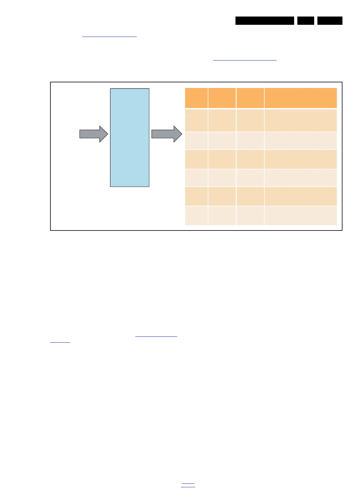
Notes to figure 7-21 TCON block diagram:
• LVDS receiver: converts the data stream back into RGB
data and SYNC signals (Vsync, Hsync, Data Enable - DE)
• ODC: Over Drive Circuit - to improve LC response
• Data Path Block: the video RGB data input to data path
block is delayed to align the column driver start pulse with
the column driver data
• Timing Control Function: generates control signals to
column drivers and row drivers (Source Enable - SOE,
Gate Enable - GOE, Gate Start Pulse - GSP).
For an overview of the TCON DC/DC converters, refer to figure
7-22 TCON DC/DC converters
.
Figure 7-22 TCON DC/DC converters
7.9.1 TCON Programming
For LGD - TCONs, the EEPROM can be programmed via
ComPair (via I
2
C communication).
For Sharp - TCONs, the data can be flashed with a “SPI
Programmer” (via SPI communication). This device has to be
ordered separately via Philips.
7.9.2 TCON Alignment
The purpose of TCON alignment is to obtain equal voltages for
both positive and negative LC polarity. This is to avoid “flicker”
and “image sticking”. For alignment, see 6.3.3 TCON/VCOM
alignment.
18770_240_100128.eps
100128
DC/DC
Controller
+12V
To Gate D rivers (Gate
Hig h Voltage)
To Gate D rivers (Gate
Low Voltag e)
Timing C ontroller IC
S upply Voltag e
Timing C ontroller IC
S upply Voltag e
S ource Driver S upply
Voltage