PDP-435PE
88
1234
1234
C
D
F
A
B
E
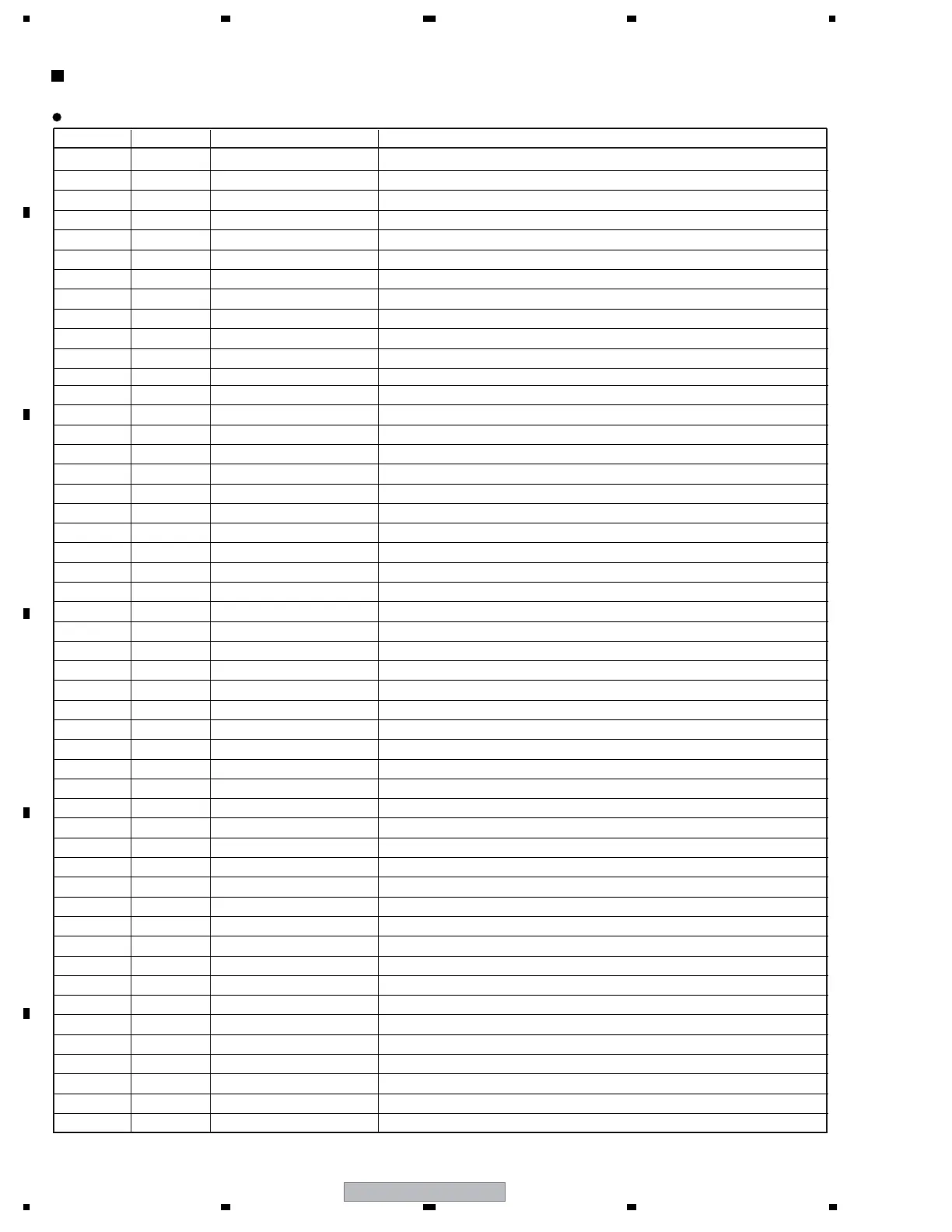
Ball No. No. Pin Name Function
AF26 51 AD4TXOUT3M Address LVDS signal output
AE26 52 AD4TXCLKOUTM Address LVDS signal output
AD26 53 AD4TXOUT2M Address LVDS signal output
AC26 54 AD4TXOUT1M Address LVDS signal output
AB26 55 AD4TXOUT0M Address LVDS signal output
AA26 56 AD5TXOUT3M Address LVDS signal output
Y26 57 AD5TXCLKOUTM Address LVDS signal output
W26 58 AD5TXOUT2M Address LVDS signal output
V26 59 AD5TXOUT1M Address LVDS signal output
U26 60 AD5TXOUT0M Address LVDS signal output
T26 61 SDIDBI_N JTAG signal
R26 62 SDIJTAG JTAG signal
P26 63 GPIO0_3 Microcomputer macro general-purpose port
N26 64 GPIO0_1 Microcomputer macro general-purpose port
M26 65 YSUSA_4 Y-Drive control signal output
L26 66 YSUSA_10 Y-Drive control signal output
K26 67 YSUSA_14 Y-Drive control signal output
J26 68 YSUSB_4 Y-Drive control signal output
H26 69 YSUSB_6 Y-Drive control signal output
G26 70 YSUSB_10 Y-Drive control signal output
F26 71 YSUSB_14 Y-Drive control signal output
E26 72 NC NC pin
D26 73 NC NC pin
C26 74 SCAN_10 Scan control signal output
B26 75 CSIOTXD Communication with microcomputer
A26 76 CSRD_N Communication with microcomputer
A25 77 CSCS_N0 Communication with microcomputer
A24 78 EXA16 Flash memory address bus
A23 79 EXA15 Flash memory address bus
A22 80 EXA14 Flash memory address bus
A21 81 EXA13 Flash memory address bus
A20 82 EXA12 Flash memory address bus
A19 83 EXA10 Flash memory address bus
A18 84 EXA7 Flash memory address bus
A17 85 EXA1 Flash memory address bus
A16 86 EXDIO_3 Flash memory data bus
A15 87 EXDIO_5 Flash memory data bus
A14 88 EXDIO_11 Flash memory data bus
A13 89 TRNSEND_O NC pin
A12 90 RBI_5 B phase signal input of R video (fifth bit)
A11 91 RBI_0 B phase signal input of R video (0 bit)
A10 92 GBI_8 B phase signal input of G video (eighth bit)
A9 93 GBI_2 B phase signal input of G video (second bit)
A8 94 BBI_6 B phase signal input of B video (sixth bit)
A7 95 BBI_0 B phase signal input of B video (0 bit)
A6 96 VDI VD signal input
A5 97 RAI_5 A phase signal input of R video (fifth bit)
A4 98 DCLKI CLK input
A3 99 GAI_4 A phase signal input of G video (fourth bit)
A2 100 BAI_9 A phase signal input of B video (ninth bit)
PDG054A (DIGITAL VIDEO ASSY : IC5401)
• PDP ASIC IC4
Pin Function (2/10)
 Loading...