53
+
-
A
MUX
10
50 k
PTC
5 M
41
42
43
44
51
52
53
54
DP2,1
DP2,2
Ω
Ω
Ω
Vreg
PR 5111
5
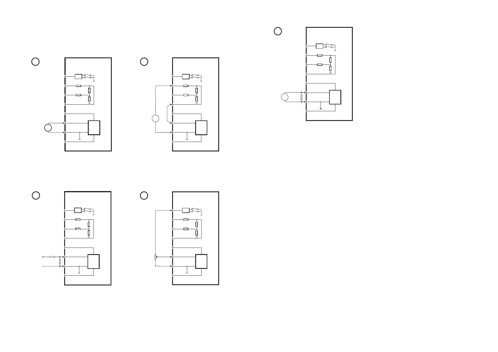
R ext.
Bipolar voltage input for current span
> ±100 mA.
External shunt is calculated as follows:
±20 mV ≤ VR
ext.
≤ ±2400 mV.
52
WIRING DIAGRAMS
FOR DC VOLTAGE INPUT
V
+
-
MUX
10
50 k
PTC
5 M
41
42
43
44
51
52
53
54
DP2,1
DP2,2
Ω
Ω
Ω
Vreg
PR 5111
1
V
-
+
MUX
10
50 k
PTC
5 M
41
42
43
44
51
52
53
54
DP2,1
DP2,2
Ω
Ω
Ω
Vreg
PR 5111
2
Bipolar voltage input for
±20 mV ≤ span ≤ ±2400 mV.
Bipolar voltage input for
±2400 mV ≤ span ≤ ±240 V.
+
-
MUX
10
50 k
PTC
5 M
41
42
43
44
51
52
53
54
DP2,1
DP2,2
Ω
Ω
Ω
Vreg
PR 5111
3
R1 ext.
R2 ext.
MUX
10
50 k
PTC
5 M
41
42
43
44
51
52
53
54
DP2,1
DP2,2
Ω
Ω
Ω
Vreg
PR 5111
4
Bipolar voltage input for span > 240 V.
External voltage divider is calculated
as follows:
±20 mV ≤ VR
2
≤ ±2400 mV.
3-wire potentiometer input.
Aux. voltage (DP2) is set at 2.5 V ref.