5G Module Series
5G-REDCAP_EVB_User_Guide 8 / 46
Figure Index
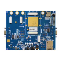
Figure 1: Top View .................................................................................................................................... 10
Figure 2: Bottom View ............................................................................................................................... 11
Figure 3: Top View for Component Placement ......................................................................................... 12
Figure 4: Bottom View for Component Placement .................................................................................... 13
Figure 5: EVB Power Supply Block Diagram ............................................................................................ 17
Figure 6: EVB Power Supply Interface ..................................................................................................... 18
Figure 7: Power Plug Design .................................................................................................................... 18
Figure 8: Connection Between the Module TE-A and EVB ....................................................................... 19
Figure 9: Connection Between Module and USB Type-C Interface .......................................................... 20
Figure 10: USB Type-C Interface .............................................................................................................. 20
Figure 11: USB-to-UART Interface ............................................................................................................ 21
Figure 12: Audio Interfaces of the EVB ..................................................................................................... 22
Figure 13: Reference Circuit Design for Loudspeaker Application ........................................................... 22
Figure 14: Reference Circuit Design for Earphone Application ................................................................. 23
Figure 15: Pin Assignment of J0503 ......................................................................................................... 23
Figure 16: Schematic of Audio Plug .......................................................................................................... 24
Figure 17: Reference Circuit Design for Handset Interface J0501 ........................................................... 25
Figure 18: Pin Assignments of J0501 ....................................................................................................... 25
Figure 19: Simplified Connector Schematic for (U)SIM Card Connectors ................................................ 26
Figure 20: Pin Assignment of (U)SIM Card Connector J0804 .................................................................. 27
Figure 21: Pin Assignment of SD Card Interface of J0701 ....................................................................... 28
Figure 22: SLIC TE-A Interface of the EVB ............................................................................................... 29
Figure 23: Connection Between Wi-Fi TE-A and EVB .............................................................................. 30
Figure 24: Connection Between PHY TE-A (PCIe Interface) and EVB ..................................................... 31
Figure 25: Connection Between PHY TE-A (SGMII/RGMII Interface) and EVB ....................................... 32
Figure 26: Antenna Interfaces ................................................................................................................... 33
Figure 27: Switches and Buttons .............................................................................................................. 35
Figure 28: Status Indicators ...................................................................................................................... 36
Figure 29: Test Points of J1202, J1203, J1204 and J1207 ....................................................................... 37
Figure 30: Test Points of J0102, J0104 and J0105 ................................................................................... 37
Figure 31: USB Ports ................................................................................................................................ 41
Figure 32: COM Port Setting Field on QCOM (USB AT Port Connection) ................................................ 41
Figure 33: USB Serial Port ........................................................................................................................ 42
Figure 34: USB Ports in PC Device Manager ........................................................................................... 43
Figure 35: Modifications and Configurations for Power Consumption ...................................................... 44
 Loading...