M10 Hardware Design
Serial port
z TXD: Send data to the RXD signal line of the DTE
z RXD: Receive data from the TXD signal line of the DTE
Debug port
z DBG_TXD: Send data to the /RXD signal line of the DTE
z DBG_RXD: Receive data from the /TXD signal line of the DTE
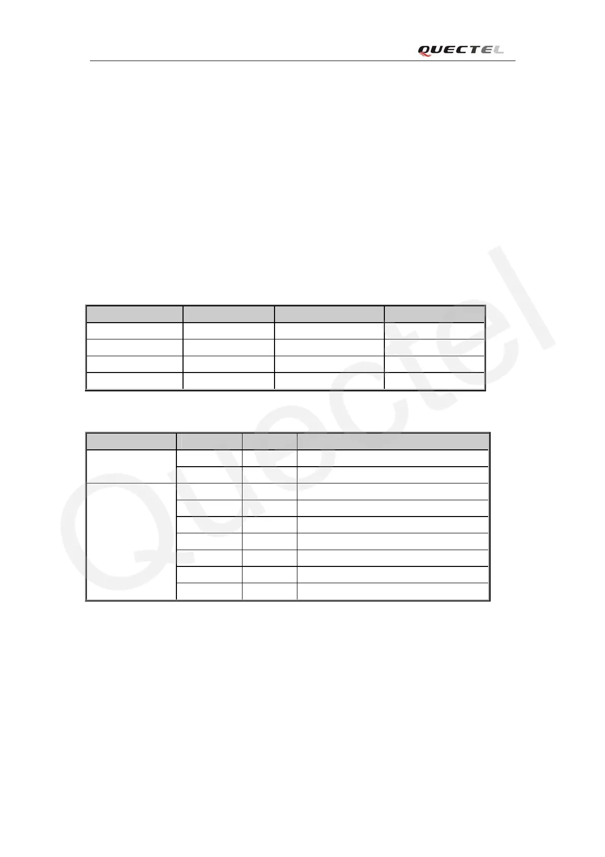
The logic levels are described in following table.
Table 9: Logic levels of the serial port and debug port
Parameter Min Max Unit
V
IL
0 0.67 V
V
IH
1.67 VDD_EXT +0.3 V
V
OL
GND 0.34 V
V
OH
2.0 VDD_EXT V
Table 10: Pin definition of the serial interfaces
Interface Name Pin Function
DBG_RXD 9 Receive data of the debug port
Debug port
DBG_TXD 10 Transmitting data of the debug port
RI 55 Ring indicator
RTS 58 Request to send
CTS 57 Clear to send
RXD 61 Receive data of the serial port
TXD 60 Transmitting data of the serial port
DTR 59 Data terminal ready
Serial port
DCD 56 Data carrier detection
M10_HD_V1.00 - 34 -