M10 Hardware Design
Voltage drop
during
transmitting burst
Normal condition, power
control level for Pout max
400 mV
Voltage ripple Normal condition, power
control level for Pout max
@ f<200kHz
@ f>200kHz
50
2
mV
POWER DOWN mode
SLEEP mode @ DRX=5
65
1.1
uA
mA
Minimum functionality mode
AT+CFUN=0
IDLE mode
SLEEP mode
AT+CFUN=4
IDLE mode
SLEEP mode
12
900
12
1
mA
uA
mA
mA
IDLE mode
GSM850/EGSM 900
DCS1800/PCS1900
12
12
mA
TALK mode
GSM850/EGSM 900
1)
DCS1800/PCS1900
2)
290/260
250/245
mA
DATA mode, GPRS (3 Rx,2Tx)
GSM850/EGSM 900
1)
DCS1800/PCS1900
2)
480/460
360/395
mA
I
VBAT
Average supply
current
DATA mode, GPRS (4 Rx,1Tx)
GSM850/EGSM 900
1)
DCS1800/PCS1900
2)
300/290
250/240
mA
Peak supply
current (during
transmission
slot every 4.6ms)
Power control level for Pout
max.
1.8 2 A
1)
Power control level PCL 5
2)
Power control level PCL 0
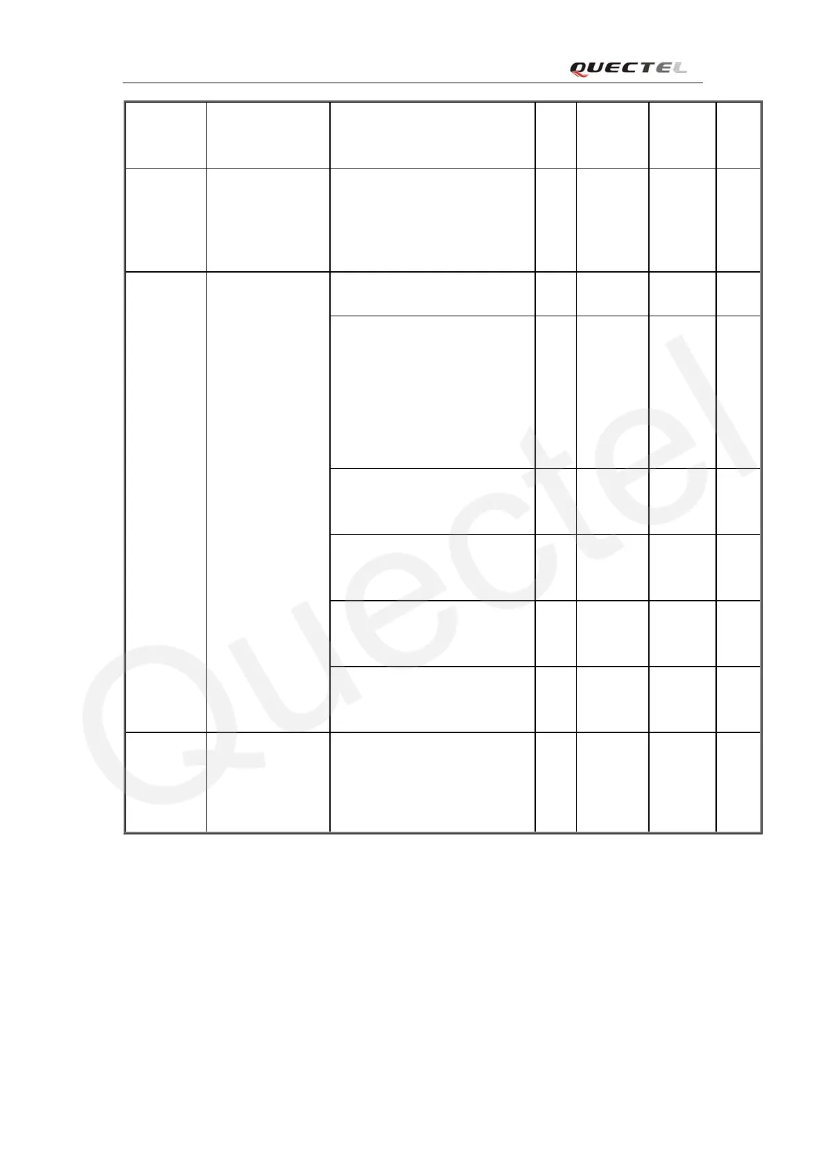
5.5 Current consumption
The values for current consumption show as following table.
Table 35: The module current consumption
M10_HD_V1.00 - 60 -
 Loading...


