M10 Hardware Design
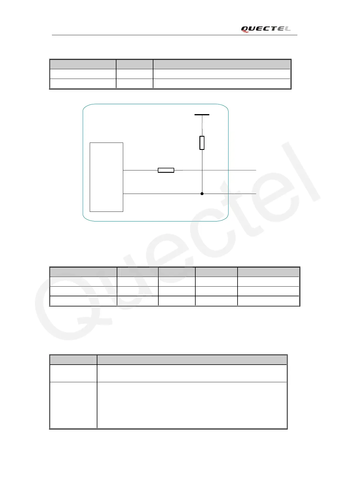
Table 21: Pin definition of the ADC
Name Pin Function
ADC0 41 Analog to digital converter.
TEMP_BAT 40 Analog to digital converter.
BASE
BAND
10K
1K
2.8V
AUXADC2
AUXADC0
ADC0
TEMP_BAT
MODULE
Figure 33: Internal circuit of the ADC
Table 22: Characteristics of the ADC
Min Typ Max Units
Voltage range 0 2.8 V
ADC Resolution 10 10 bits
ADC accuracy 2.7 mV
3.15 Behaviors of the RI
Table 23: Behaviours of the RI
State RI respond
Standby HIGH
Voice calling Change LOW, then:
(1)Change to HIGH when establish calling.
(2)Use AT command ATH, the RI pin changes to HIGH.
(3)Sender hangs up, change to HIGH.
(4) Change to HIGH when SMS received.
M10_HD_V1.00 - 51 -