Automotive Module Series
AG525R-GL QuecOpen
Hardware Design
AG525R-GL_QuecOpen_Hardware_Design 68 / 104
1. The input voltage for each ADC interface must not exceed its corresponding voltage range.
2. It is prohibited to supply any voltage to ADC pins when VBAT is removed.
3. It is recommended to use resistor divider circuit for ADC application.
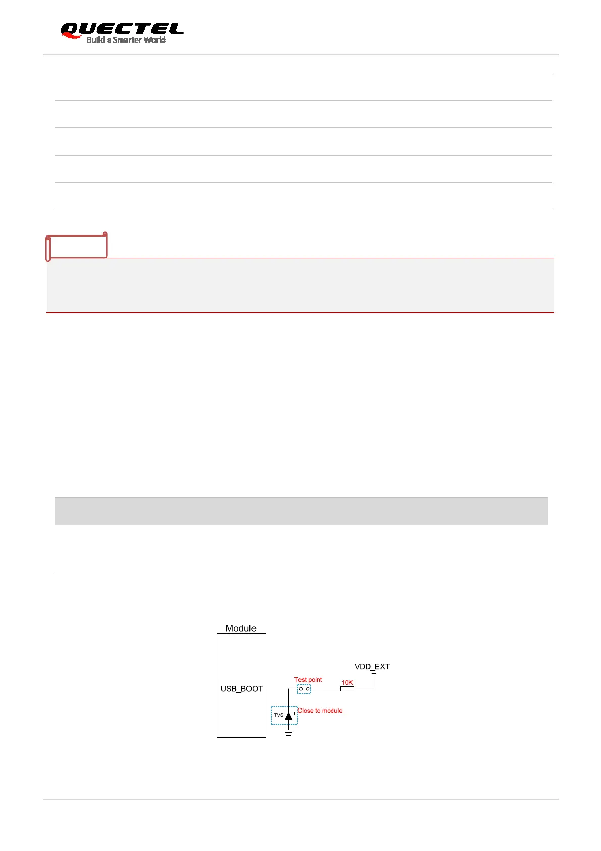
3.18. USB_BOOT Interface
The module provides a USB_BOOT pin. Pulling up the USB_BOOT to VDD_EXT before powering on the
module will force the module into emergency download mode when powered on. In emergency download
mode, the module supports firmware upgrade over USB 2.0 interface.
Table 26: Pin Definition of USB_BOOT Interface
Pin Name Pin No. I/O Description Comment
USB_BOOT 83 DI
Force the module into emergency
download mode
1.8 V power domain.
Active high.
If unused, keep it open.
The following figure shows a reference circuit of USB_BOOT interface.
Figure 30: Reference Circuit of USB_BOOT Interface
ADC0 Voltage Range 0 1.875 V
ADC1 Voltage Range 0 1.875 V
ADC2 Voltage Range 0 1.875 V
ADC Resolution 14 bits
ADC Sample Rate 4.8 MHz
NOTES
 Loading...


