Renesas RA Family EK-RA4E2 v1 – User's Manual
R20UT5175EG0300 Rev. 3.00 Page 15 of 30
Feb.27.23
5.1.2 Power Supply Considerations
The on-board LDO regulator which supplies +3.3 V has a built-in current limit of 2.0 A. Make sure the total
current required by the RA MCU, any active on-board features, and any connected peripheral devices does
not exceed this limit.
Note: The total current available from a typical USB host is 500 mA maximum. Depending on the
configuration of the kit, multiple power sources may be required.
5.1.3 Power-up Behavior
When powered, the white LED near the center of the board (the “dash” in the EK-RA4E2 name) will light up.
For more details on initial power up behavior, see the EK-RA4E2 Quick Start Guide.
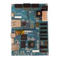
5.2 Debug and Trace
The EK-RA4E2 board supports the following three debug modes.
Table 3. Debug Modes
(the device that
connects to the
(the device that
is being
Interface/Protocol
debugging tools
or 10-pin connector
(J13)
MCU
either 20-pin connector
(J20)
or 10-pin connector
Notes:
• See Table 5 for the Debug USB connector pin definitions.
• See Table 8 for the 20-pin JTAG connector pin definitions.
• See Table 9 for the 10-pin JTAG connector pin definitions.
The following table summarizes the jumper setting for each of the debug modes.
Table 4. Jumper Connection Summary for Different Debug Modes
Jumpers on pins 1-2, 3-4, 5-6, 7-8
Jumpers on pins 1-2, 3-4, 5-6, 7-8
5.2.1 Debug On-Board
The on-board debug functionality is provided using Renesas RA4M2 Debug MCU and SEGGER J-Link
®
firmware. Debug USB micro-B connector (J10) connects the RA4M2 Debug MCU to an external USB Full
Speed Host, allowing re-programming and debugging of the target RA MCU firmware. This connection is the
default debug mode for the EK-RA4E2 board.
The RA4M2 debug MCU connects to the target RA MCU using the SWD interface.
Table 5. Debug USB Connector
USB ID, jack internal switch, cable inserted