RZ/A2M SUB Board RTK79210XXB00000BE 2. Function specifications
R20UT4398EJ0100 Rev.1.00 2-38
2018.10.11
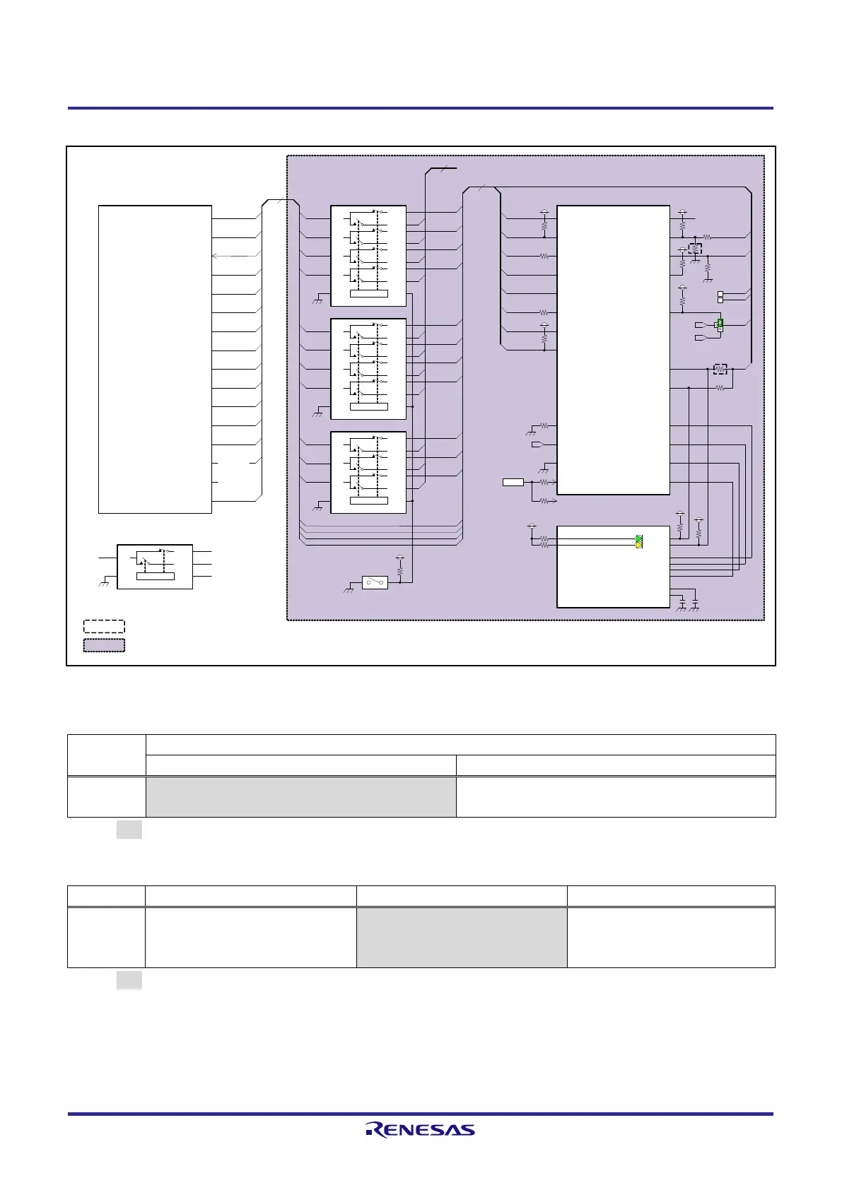
Figure 2.13.2 LAN Interface (channel 1) Block Diagram
Table 2.13.4 Function Setting Table of DIP Switch SW6-5 for System Setting
P3_[5 :1] and PH_5, PK_[4 :0] are used as Ethernet
PHY2 control pins (default settings).
P3_[5 :1] and PH_5, PK_[4 :0] are used as FLCTL
pins.
[Note] indicates setting functions.
Table 2.13.5 Function Setting Table of Jumper JP1
PJ_1 is used as Ethernet PHY1
signal interrupt pin.
PJ_1 is used as Ethernet PHY2
signal interrupt pin.
PJ_1 is used as IRQ0 switch
(SW3) interrupt pin (default
setting).
[Note] indicates setting functions.
PK_4
15
PK_0
PK_3
P3_4
PK_2
P3_1
P3_2
P3_5
P3_3
PK_1
LINK
WOL
PH_5
Ether2 / NAND(U14)
TXD0
EXOUT
TXDEN
RXD1
LINK
WOL#
Ether2 / NAND(U17)
MUXOE# S
4A
4B1
4B2
3A
3B1
3B2
2A
2B1
2B2
1A
1B1
1B2
MUXOE# S
4A
4B1
4B2
3A
3B1
3B2
2A
2B1
2B2
1A
1B1
1B2
Ether2 / NAND(U19)
MUXOE# S
3A
3B1
3B2
2A
2B1
2B2
1A
1B1
1B2
ON(L):A=B1, OFF(H):A=B2
MDC
CRSDV
MDIO
RXER
15
11
To NAND flash memory
P3_3
P3_2
P3_4
P3_1
PK_1
PH_5
PK_0
P3_5
PK_2
PK_3
TXD1
REFCLK
INT#
3.3V
DIP
SW6-5
RXD0
PK_4
ON
MDIO
MDC
TXD[1:0]
TXDEN
REFCLK
RXD1
RXER
CRSDV
RES#
3.3V
INT#
RXD0
3.3V
NC
3.3V
CLK
50MHz
(X4)
To EthernetPHY1
RJ45(CN9)3.3V
NC
3.3V
WOL#
IRQ0
WOL1
TD+
TD-
RD+
RD-
CT1
CT2
LED-G
LED-Y
EthernetPHY2(U28)
MDC
MDIO
MDI+[0]
MDI-[0]
Transmit output
Receive input
MDI+[1]
MDI-[1]
TXD[1:0]
RXD[1]
TXC
TXEN
CRS_DV
RXER / FXEN
LED0 / PHYAD[0]
INTB
LED1 / PHYAD[1]
RXD[0]
LI/O/PD (1:Fiber, 0:UTP)
LI/PU
RXD[3] / CLK_CTL
LI/O/PD (1:REFCLK input, 0:output)
LI/PD
LI/O/PD (1:WOL, 0:LED)
RXDV
LI/O/PD (1:RMII, 0:MII)
PHYRSTB
CKXTAL 1
CKXTAL 2
RXD[2]
PMEB
TXD[3:2]
COL
RXC
TXER
IO/PD
I/PU
I/PD
I/PD
IO/PU
O/PD
O/PD
O/OD
I/PD
O/PD
I/PD
O/PD
O/PD
RSET
3.3V
WOL#
RZ/A2M (U1)
PK_4 / ET1_RXD0/RMII1_RXD0 /
NAF7
P3_5 / ET1_RXD1/RMII1_RXD1 /
FCLE
P3_1 / ET1_RXER/RMII1_RXER /
FALE
P3_2 / ET1_CRS/RMII1_CRSDV /
FRE
P3_3 / ET1_MDC/ FWE
P3_4 / ET1_MDIO/ FRB
P3_0 / ET1_LINKSTA
PK_1 / ET1_TXD0/RMII1_TXD0 /
NAF4
PK_3 / ET1_RXCLK/REF50CK1 /
NAF6
PH_5 / NAF2 / ET1_EXOUT
PK_2 / ET1_TXD1/RMII1_TXD1 /
NAF5
PH_6 / ET1_WOL
PK_0 / ET1_TXEN/RMII1_TXDEN /
NAF3
PL_1 / MD_CLK / IRQ5
PJ_1 / IRQ0 (DSTBY release)
LINK
EXOUT
WOL
TP1
TP2
3
1
WOL
3.3V
3.3V
Note: Red text indicates a function used.
:Indicates a function not implemented.
:Indicates a SUB board.
JP1
JP2
2.49k±1%
PD_0
(IRQ input # / system
setting selection)
MUXOE# S
2A
2B1
2B2
【C】
L:A=B1, H:A=B2
IRQ input /
System settings (U6)
【A】
INT#
To CPU board SW1
【B】
【A】
【C】
【B】
Low
 Loading...


