Chapter 3 – SD Card Interface Description
Revision 2.2 SD Card Product Manual
© 2004 SanDisk Corporation 3-10 12/08/04
Parameter Symbol Min Max Unit Remark
Clock (CLK) – all values referred to min. V
IH
and max. V
IL
Output delay time during Data
Transfer mode
t
OSU
0 14 ns C
L
< 25 pF (1 card)
Output delay time during
Identification mode
t
ODLY
0 50 ns C
L
< 25 pF (1 card)
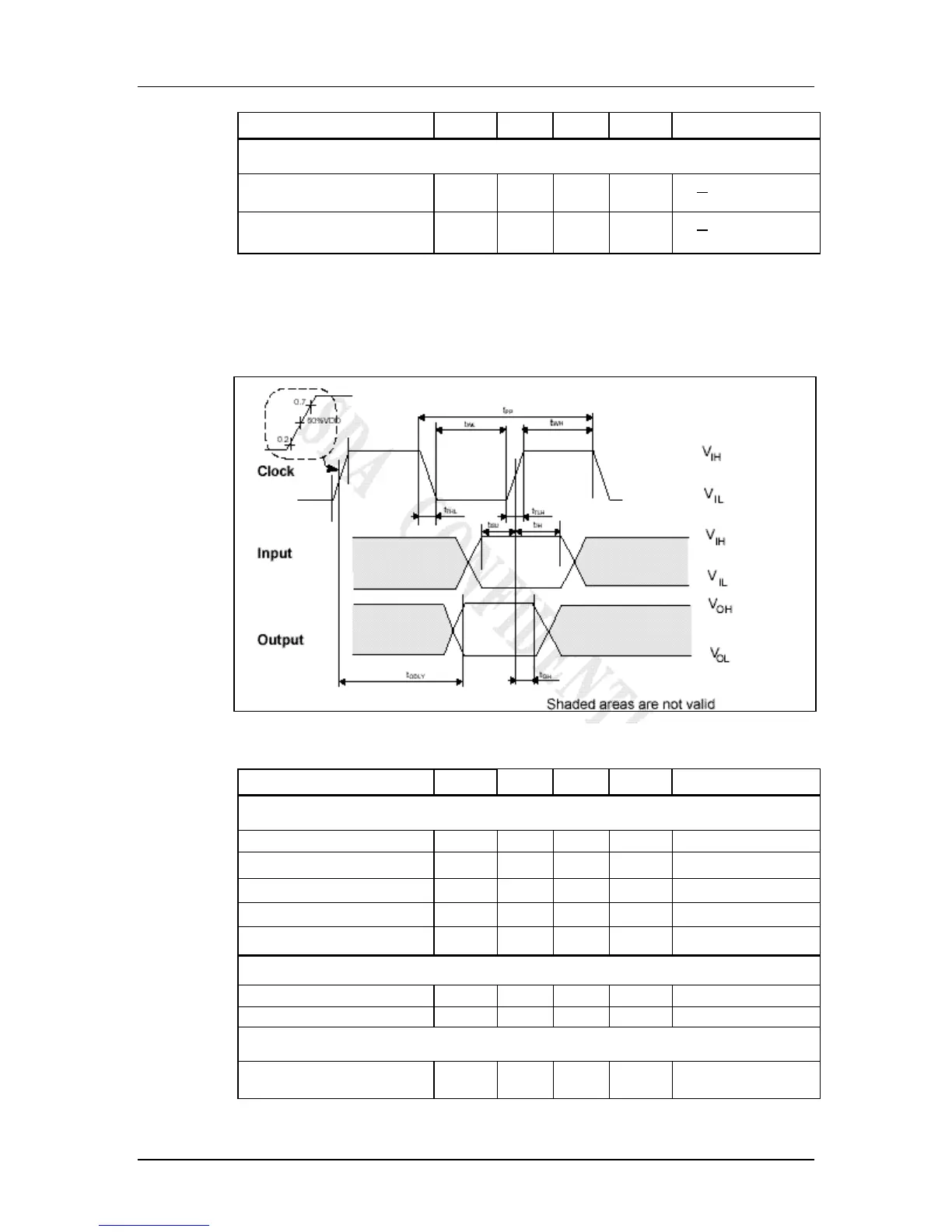
3.4.7 Bus Timing (high-speed mode)
High-speed mode dataIn/dataOut timing is illustrated in Figure 3-8; bus timing parameter
values are shown in Table 3-8.
Figure 3-8 Data In/Out Referenced to Clock Timing (high-speed)
Table 3-8 Bus Timing Parameter Values (high-speed)
Parameter Symbol Min Max Unit Remark
Clock (CLK) – all values referred to min. V
IH
and max. V
IL
Clock Freq. Data Transfer Mode f
PP
0 50 MHz
Clock Low Time t
WL
7 --- ns
Clock High Time t
WH
7 --- ns
Clock Rise Time t
TLH
--- 3 ns
Clock Fall Time t
THL
--- 3 ns
Inputs CMD, DAT – referenced to CLK
Input setup time t
ISU
6 --- ns
Input hold time t
IH
2 --- ns
Outputs CMD, DAT – referenced to CLK
Output delay time during Data
Transfer mode
t
ODLY
--- 14 ns
 Loading...