LC-52XS1E/RU/LC-65XS1E/RU
5 – 13
Pin No. Pin Name I/O Pin Function
70, 71 TA1+, TA1-
O
The 1st Link.
The 1st pixel output data when Dual-Link.
68, 69 TB1+, TB1-
64, 65 TC1+, TC1-
58, 59 TD1+, TD1-
56, 57 TE1+, TE1-
62, 63 TCLK1+, TCLK1- O LVDS Clock Out for 1st and 2nd Link.
52, 53 TA2+, TA2-
O
The 2nd Link.
These pins are disabled when Single Link.
50, 51 TB2+, TB2-
46, 47 TC2+, TC2-
40, 41 TD2+, TD2-
38, 39 TE2+, TE2-
44, 45 TCLK2+, TCLK2- O Additional LVDS Clock Out. Identical to TCLK1+,-. No connect if not used.
87 - 84,
81 - 76
R19 ~R10
I
The 1st Pixel Data Inputs.
R1 [9 : 0]
99 - 95,
92 - 88
G19 ~G10 G1 [9 :0]
112 -110,
108 -106,
103 - 100
B19 ~B10 B1 [9 :0]
124 - 115 R29 ~R20
I
The 2nd Pixel Data Inputs.
R2 [9 : 0]
136 - 127 G29 ~G20 G2 [9 : 0]
6, 5, 2, 1,
144 - 139
B29 ~B20 B2 [9 : 0]
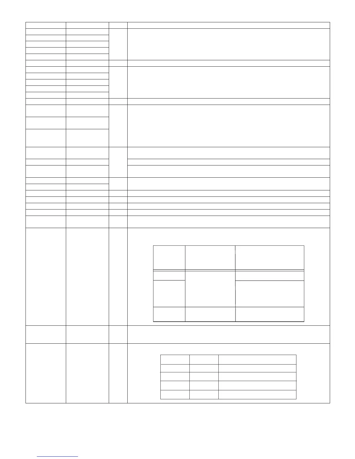
17, 18 CONT11,CONT12
I
CONTROL Data Inputs.
19, 20 CONT21,CONT22
9 DE I Data Enable Input.
8 VSYNC I Vsync Input.
7 HSYNC I Hsync Input.
15 CLKIN I Clock Input.
21 R/F
I
Input Clock Triggering Edge Select.
H: Rising edge, L: Falling edge
22 RS I The use of these multi-function depends on input voltage of RS pin.
24 MAP I LVDS mapping table select.
H: Mapping Mode1
L: Mapping Mode2
25, 26 MODE1, MODE0 I Pixel Data Mode.
Input voltage
of RS pin
VCC
0.6~1.4V
GND
LVDS output
Swing Control
Normal Swing
VOD=350mV(typ)
Reduced Swing
VOD=200mV(typ)
TTL/CMOS Input
VIH/VIL Control for
Small Swing Input
VIH/VIL is fixed
Support Small Swing Input
VIH/VIL depends on
input voltage of RS pin
See VIH/VIL Spec
VIH/VIL is fixed
MODE 1
MODE 2
MODE
L
L
HL
L
H
H
H
Dual Link (Dual-in/Dual-out)
Dual Link (Single-in/Dual-out)
Single Link (Dual-in/Single-out)
Single Link (Single-in/Single-out)