Table 1-13 Allocation of the LVDS display interface
Connector Pin Name Type Meaning
1/2 P5V_D_fused VO +5 V display supply voltage (fused in PCU/
TCU)
3 RXIN0-
I LVDS input signal
Bit 0 (-)
4 RXIN0+ Bit 0 (+)
5/6 P3V3_D_fused VO +3.3 V display supply voltage (fused in PCU/
TCU)
7 RXIN1-
I LVDS input signal
Bit 1 (-)
8 RXIN1+ Bit 1 (+)
9/10 GND - System ground (reference potential)
11 RXIN2-
I LVDS input signal
Bit 2 (-)
12 RXIN2+ Bit 2 (+)
13/14 GND - System ground (reference potential)
15 RXCLKIN-
O LVDS cycle clock signal
(-)
16 RXCLKIN+ (+)
17/18 GND
-
System ground (reference potential)
19/20 N.C. Not connected
LVDS display interface channel 2
Used for expanding the LVDS display interface channel 1 to control TFT displays with 1280 x
1024 pixels (SXGA).
Associated interface cable: K3
Connector type: 2 x 10-pin socket connector
Table 1-14 Allocation of the LVDS display interface
Connector Pin Name Type Meaning
1/2 GND - System ground (reference potential)
3 RXIN10-
I
LVDS input signal Bit 0 (-)
4 RXIN10+ Bit 0 (+)
5/6 GND - System ground (reference potential)
7 RXIN1-
I
LVDS input signal Bit 1 (-)
8 RXIN1+ Bit 1 (+)
9/10 GND - System ground (reference potential)
11 RXIN2-
I
LVDS input signal Bit 2 (-)
12 RXIN2+ Bit 2 (+)
13/14 GND V Ground
15 RXCLKIN-
O
LVDS cycle clock sig‐
nal
(-)
16 RXCLKIN+ (+)
17 GND V Ground
18-20 P12VF VO +12 V fused
General information and networking
1.3 Connecting
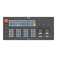
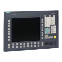
Operator panel front: OP 010
Manual, 07/2018, A5E36371538B 29
 Loading...