SIM900 Hardware Design
C
A
C
B
VBAT
+
Figure 3: Reference circuit of the VBAT input
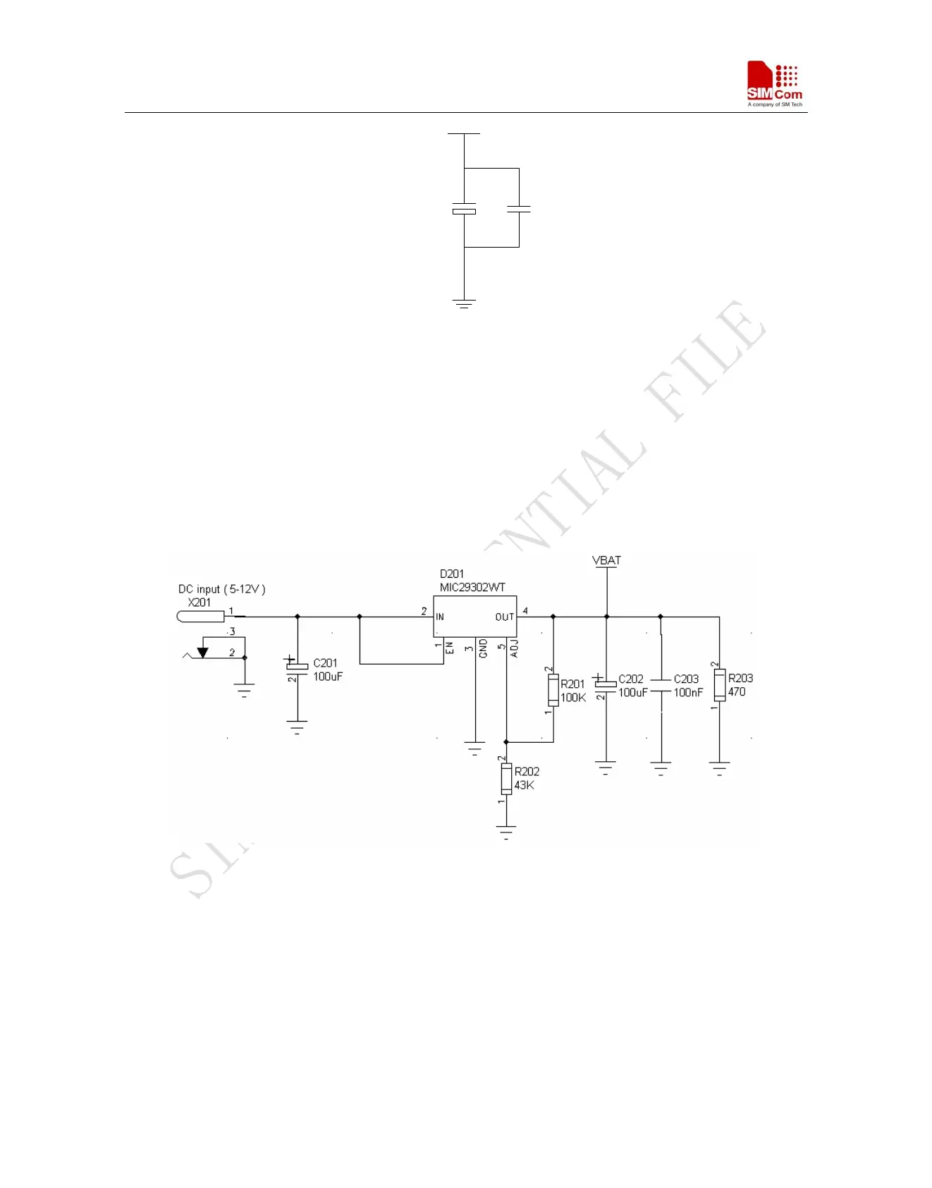
The circuit design of the power supply depends strongly upon the power source where this power is drained. The
following figure is the reference design of +5V input source power supply. The designed output for the power
supply is 4.1V, thus a linear regulator can be used. If there’s a big difference between the input source and the
desired output (VBAT), a switching converter power supply will be preferable because of its better efficiency
especially with the 2A peak current in burst mode of the module.
The single 3.6V Li-Ion cell battery type can be connected to the power supply of the SIM900 VBAT directly. But
the Ni_Cd or Ni_MH battery types must be used carefully, since their maximum voltage can rise over the absolute
maximum voltage for the module and damage it.
Figure 4: Reference circuit of the source power supply input
The following figure is the VBAT voltage ripple wave at the maximum power transmit phase, the test condition is
VBAT=4.0V, VBAT maximum output current =2A, C
A
=100µF tantalum capacitor (ESR=0.7Ω) and C
B
=1µF.
SIM900_HD_V1.05 06.23.2010
22