Do you have a question about the Skyworks Si5341 and is the answer not in the manual?
Explains using ClockBuilder Pro and register map for device configuration.
Compares different family members of the clock generator.
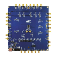
Lists available software tools and support resources for the device.
Details the five classes of dividers within the Si5341/40.
Describes the device power-up and initialization sequence and reset types.
Explains the process of programming non-volatile memory.
Details crystal and clock input configurations for XA/XB pins.
Describes single-ended or differential clock inputs on IN2, IN1, IN0 pins.
Explains how to handle and disable unused input pins.
Covers selecting the active clock input via pins or register.
Details fault indicators for loss of signal and loss of lock for the PLL.
Describes the differential and LVCMOS output capabilities of Si5341/40.
Provides guidelines for minimizing crosstalk and optimizing output jitter.
Details programmable output signal formats like LVDS, LVPECL, HCSL, and LVCMOS.
Explains how N dividers connect to R dividers and output drivers.
Describes the zero delay mode for consistent input-to-output delay.
Explains digital control of N dividers for real-time frequency changes.
Details using the M divider for small frequency changes in ppm.
Outlines special write sequences for dynamic PLL changes in older revisions.
Details preamble and postamble values for Revision D and later devices.
Describes the I2C serial interface operation and configuration.
Details the SPI serial interface operation and configurations.
Provides layout guidelines for the 64-pin Si5341 device.
Details layout recommendations for the 44-pin Si5340 device.
Lists features for powering down functions to minimize consumption.
Offers recommendations for power supply filtering and capacitors.
Emphasizes proper grounding for electrical and thermal performance.
Explains the importance of power supply sequencing for phase-aligned outputs.
Describes "base" devices that require configuration for operation.
Explains factory-programmed devices with custom OPNs.
Provides an overview of register pages and default settings.
Lists register map details specific to the Si5341 device.
Lists register map details specific to the Si5340 device.
| Number of Outputs | 4 |
|---|---|
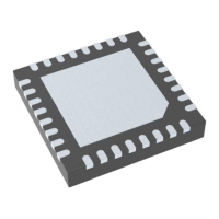
| Package Type | QFN |
| Package | 32-pin QFN |
| Operating Temperature Range | -40°C to 85°C |
| Category | Clock Generator |
| Power Supply Voltage | 3.3 V |
| Output Format | LVPECL |