11. Crystal and Device Circuit Layout Recommendations
The main layout issues that should be carefully considered include the following:
• Number and size of the ground vias for the Epad (see Section 12.3 Grounding Vias for details)
• Output clock trace routing
• Input clock trace routing
• Control and Status signals to input or output clock trace coupling
• XTAL signal coupling
• XTAL layout
If the application uses a crystal for the XAXB inputs a shield should be placed underneath the crystal connected to the X1 and X2 pins
(4 and 7) to provide the best possible performance. The shield should not be connected to the ground plane and the planes underneath
should have as little under the shield as possible. It may be difficult to do this for all the layers, but it is important to do this for the layers
that are closest to the shield.
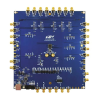
Refer to the High Performance Clock Generator Kits on the Clock Development Tools web page for the Si5341-EVB and Si5340-EVB
schematics, layout, and BOM files.
11.1 64-Pin QFN Si5341 Layout Recommendations
This section details the recommended guidelines for the crystal layout of the 64-pin Si5341 device using an example 8-layer PCB.
Following are descriptions of each of the eight layers.
• Layer 1: device layer, with low speed CMOS control/status signals, ground flooded
• Layer 2: crystal shield
• Layer 3: ground plane
• Layer 4: power distribution
• Layer 5: power routing layer
• Layer 6: input clocks
• Layer 7: output clocks layer
• Layer 8: ground layer
Figure 11.1 64-pin Si5341 Crystal Layout Recommendations Top Layer (Layer 1) on page 47 is the top layer layout of the Si5341
device mounted on the top PCB layer. This particular layout was designed to implement either a crystal or an external oscillator as the
XAXB reference. The crystal/ oscillator area is outlined with the white box around it. In this case, the top layer is flooded with ground.
Note that this layout has a resistor in series with each pin of the crystal. In typical applications, these resistors should be removed.
11.1.1 Si5341 Applications without a Crystal
If the application does not use a crystal, then the X1 and X2 pins should be left as “no connect” and should not be tied to ground. In
addition, there is no need for a crystal shield or the voids underneath the shield. If there is a differential external clock input on XAXB
there should be a termination circuit near the XA and XB pins. This termination circuit should be two 50 Ω resistors and one 0.1 μF
cap connected in the same manner as on the other clock inputs (IN0, IN1 and IN2). See Figure 4.1 Crystal Resonator and External
Reference Clock Connection Options on page 16. The clock input on XAXB must be ac-coupled. Care should be taken to keep all
clock inputs well isolated from each other as well as any other dynamic signal. For LVCMOS or clipped sine wave inputs on XAXB, see
Figure 4.1 Crystal Resonator and External Reference Clock Connection Options on page 16.
Si5341, Si5340 Rev D Family Reference Manual • Crystal and Device Circuit Layout Recommendations
Skyworks Solutions, Inc. • Phone [781] 376-3000 • Fax [781] 376-3100 • sales@skyworksinc.com • www.skyworksinc.com
46 Rev. 1.3 • Skyworks Proprietary Information • Products and Product Information are Subject to Change Without Notice • July 26, 2021 46