4.4 Reference Input Selection (IN0, IN1, IN2, XA/XB)
The active clock input is selected using the IN_SEL1,0 pins or by register control. The register bit IN_SEL_REGCTRL determines input
selection as pin or register selectable. If the selected input does not have a clock, all output clocks will be shut off.
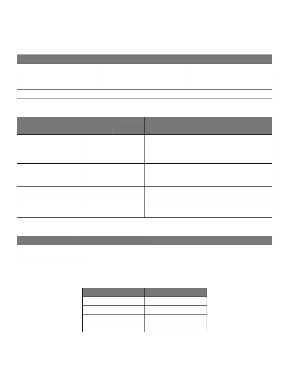
Table 4.1. Manual Input Selection Using IN_SEL[1:0] Pins
IN_SEL[1:0] Selected Input
0 0 IN0
0 1 IN1
1 0 IN2
1 1 XA/XB
Table 4.2. Input Control Registers
Register Name
Hex Address [Bit Field]
Function
Si5341 Si5340
XAXB_FREQ_OFFSET 0202[7:0]–0205[7:0]
Adjusts for crystal load capacitance mismatch causing oscillation
frequency errors up to ±1000 ppm. This word is in 2s complement
format.
The XAXB_FREQ_OFFSET word is added to the M divider nu-
merator.
XAXB_EXTCLK_EN 090E[0]
Selects between the XTAL or external reference clock on the
XA/XB pins. Default is 0, XTAL. Set to 1 to use an external refer-
ence oscillator
IN_SEL_REGCTRL 0021[0] Determines pin or register clock input selection.
IN_SEL 0021[2:1] Selects the input when in register input selection mode.
IN_EN 0949[3:0]
Allows enabling/disabling IN0, IN1, IN2 and FB_IN when not in
use.
Table 4.3. XAXB Pre-Scale Divide Ratio Register
Setting Name Hex Address [Bit Field] Function
PXAXB 0x0206[1:0] Sets the XAXB input divider value according to the table be-
low.
The following table lists the values, along with the corresponding divider ratio.
Table 4.4. XAXB Pre-Scale Divide Values
Value (Decimal) PXAXB Divider Value
0 1
1 2
2 4
3 8
Si5341, Si5340 Rev D Family Reference Manual • Clock Inputs
Skyworks Solutions, Inc. • Phone [781] 376-3000 • Fax [781] 376-3100 • sales@skyworksinc.com • www.skyworksinc.com
18 Rev. 1.3 • Skyworks Proprietary Information • Products and Product Information are Subject to Change Without Notice • July 26, 2021 18