5.3.7 LVCMOS Output Polarity
When a driver is configured as an LVCMOS output it generates a clock signal on both pins (OUTx and OUTxb). By default the clock on
the OUTxb pin is generated with the opposite polarity (complementary) with the clock on the OUTx pin. The polarity of these clocks is
configurable enabling in-phase clock generation and/or inverted polarity with respect to other output drivers.
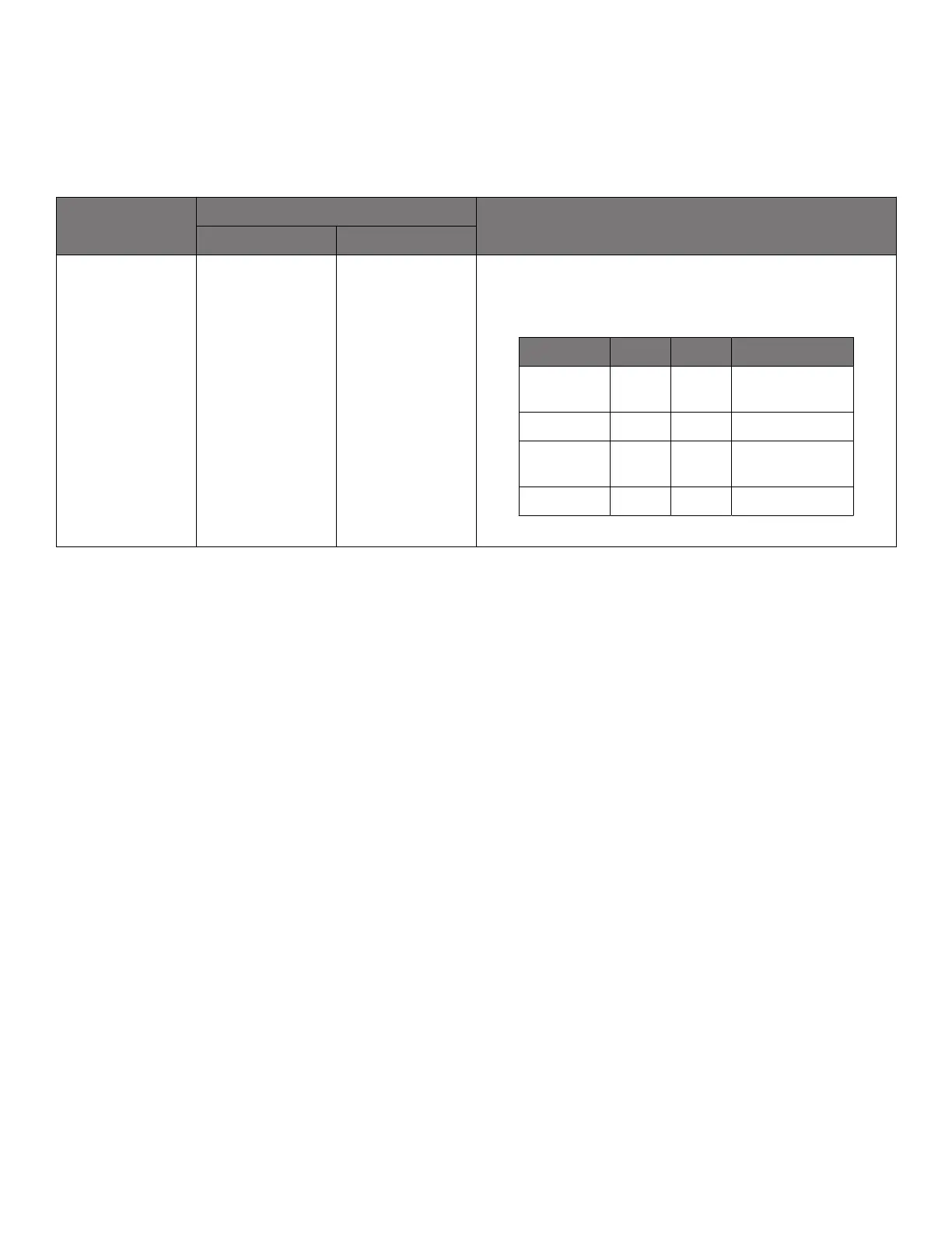
Table 5.6. LVCMOS Output Polarity Control Registers
Setting Name Hex Address [Bit Field] Function
Si5341 Si5340
OUT0_INV
OUT1_INV
OUT2_INV
OUT3_INV
OUT4_INV
OUT5_INV
OUT6_INV
OUT7_INV
OUT8_INV
OUT9_INV
010B[7:6]
0110[7:6]
0115[7:6]
011A[7:6]
011F[7:6]
0124[7:6]
0129[7:6]
012E[7:6]
0133[7:6]
0138[7:6]
0115[7:6]
011A[7:6]
0129[7:6]
012E[7:6]
—
—
—
—
—
—
Controls output polarity of the OUTx and OUTxb pins when in
LVCMOS mode. Selections are as follows:
OUTx_INV OUTx OUTxb Comment
0 0 CLK CLK
Both in phase
(default)
0 1 CLK CLKb OUTxb inverted
1 0 CLKb CLKb
OUTx and OUTxb
inverted
1 1 CLKb CLK OUTx inverted
Si5341, Si5340 Rev D Family Reference Manual • Output Clocks
Skyworks Solutions, Inc. • Phone [781] 376-3000 • Fax [781] 376-3100 • sales@skyworksinc.com • www.skyworksinc.com
28 Rev. 1.3 • Skyworks Proprietary Information • Products and Product Information are Subject to Change Without Notice • July 26, 2021 28