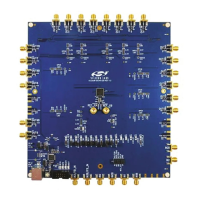
CS
SCLK
SDI
SDO
SDIO
4-Wire
3-Wire
‘Read Data’ or ‘Read Data + Address Increment’
Command
Previous
Command
Next
Command
1
0
01234567
1
0
6
7
01234567
1
0
01234567
6
7
6
7
01234567
Si5341/40Host
Si5341/40Host
Don’t Care
High Impedance
Read Data instruction
Read byte @ base address + 1
> 2.0
SCLK
Periods
> 2.0
SCLK
Periods
Figure 8.11. SPI “Read Data” and “Read Data + Address Increment” Instruction Timing
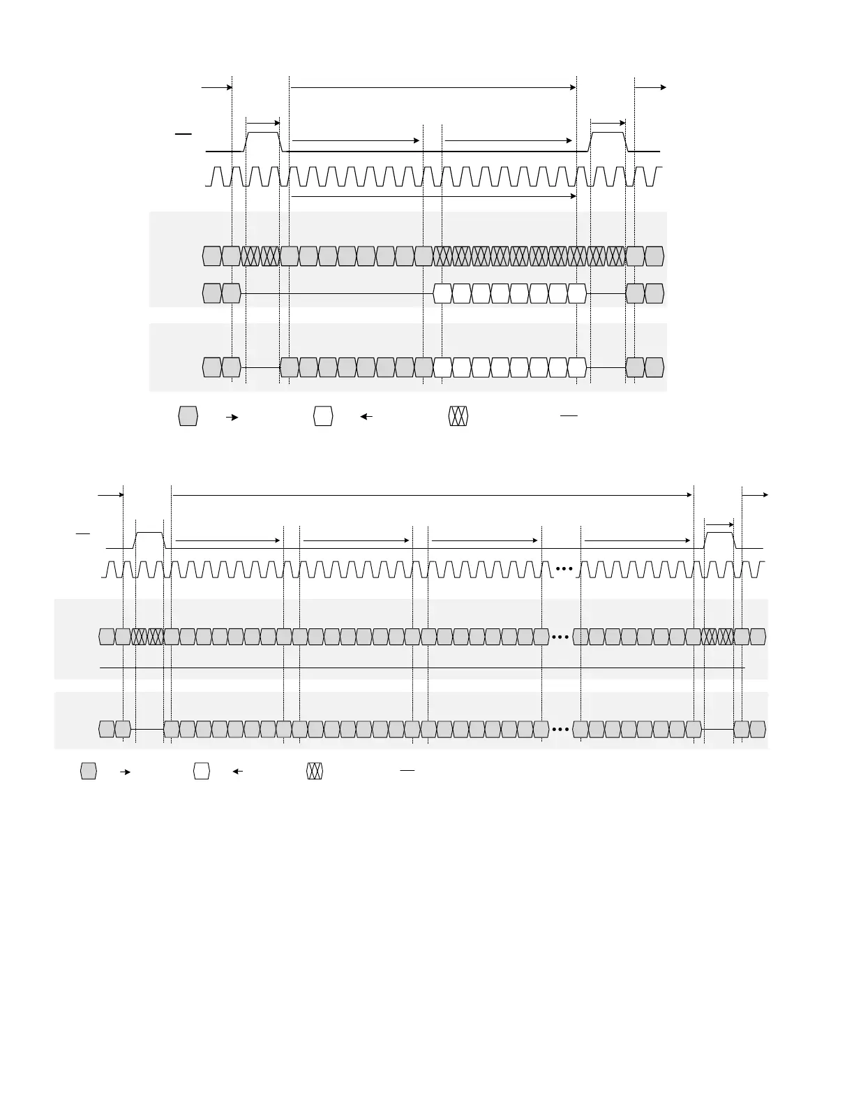
Burst Write Instruction Base address
CS
SCLK
SDO
SDIO
4-Wire
n
th
data byte @ base address +n
3-Wire
‘Burst Data Write’ Command
Previous
Command
SDI
1
0
01234567
0123456 0123456 01234567
1
0
01234567
0123456 0123456 0123456
Si5341/40Host
Si5341/40Host
Don’t Care
High Impedance
1
st
data byte @ base address
6
Next
Command
6
7
7
7
7
7 7 7
> 2.0
SCLK
Periods
> 2.0
SCLK
Periods
Note that for all SPI communication the chip select (CS) must be high for the minimum time period between commands. When chip
select goes high it indicates the termination of the command. The SCLK can be turned off between commands, particularly if there are
very long delays between commands.
Figure 8.12. SPI “Burst Data Write” Instruction Timing
Si5341, Si5340 Rev D Family Reference Manual • Serial Interface
Skyworks Solutions, Inc. • Phone [781] 376-3000 • Fax [781] 376-3100 • sales@skyworksinc.com • www.skyworksinc.com
43 Rev. 1.3 • Skyworks Proprietary Information • Products and Product Information are Subject to Change Without Notice • July 26, 2021 43