– 3 –
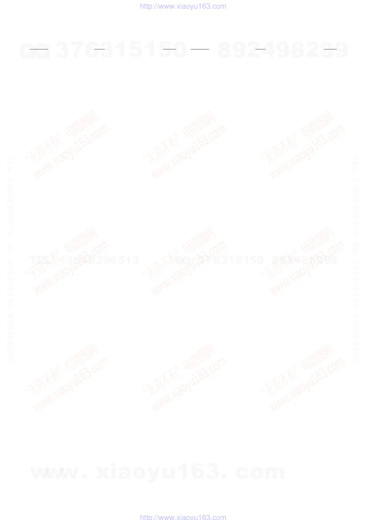
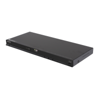
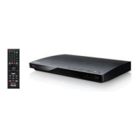
BDP-BX2/S360
TABLE OF CONTENTS
Section Title Page Section Title Page
1. SERVICE NOTE
1-1. Disc Removal Procedure If The Tray Cannot Be
Ejected (Forced Ejection) ............................................. 1-1
1-2. Work when optical device are replaced ........................ 1-1
1-3. Test Disc ....................................................................... 1-2
1-3-1. Operation and Display ............................................. 1-2
2. DISASSEMBLY
2-1. Disassembly Flow ........................................................ 2-1
2-2. Upper Case .................................................................. 2-1
2-3. Front Panel Assy .......................................................... 2-2
2-4. BD Drive ....................................................................... 2-2
2-5. Rear Panel Block.......................................................... 2-3
2-6. MB-127 Board .............................................................. 2-3
2-7. Switching Regulator ..................................................... 2-4
2-11. Circuit Boards Location ................................................ 2-4
3. BLOCK DIAGRAMS
3-1. Overall Block Diagram.................................................. 3-1
3-2. DSP Block Diagram ...................................................... 3-2
3-3. AV OUT Block Diagram ................................................ 3-3
3-4. USB/ETHER, FL Block Diagram .................................. 3-4
3-5. Power Block Diagram (1/2) .......................................... 3-5
3-6. Power Block Diagram (2/2) .......................................... 3-6
4. SCHEMATIC DIAGRAMS
4-1. This Note Is Common For Schematic Diagrams .......... 4-1
4-2. Frame Schematic Diagram........................................... 4-2
4-3. FL-193 Board (SWITCH) Schematic Diagram ............. 4-3
4-4. FR-301 Board (FL DRIVER) Schematic Diagram ........ 4-4
4-5. MB-127 Board (MC10121F1 DDR2-A)
Schematic Diagram (1/14)............................................ 4-5
4-6. MB-127 Board (MC10121F1 DDR2-B)
Schematic Diagram (2/14)............................................ 4-6
4-7. MB-127 Board (POWER1)
Schematic Diagram (3/14)............................................ 4-7
4-8. MB-127 Board (CLK/POWER2)
Schematic Diagram (4/14)............................................ 4-8
4-9. MB-127 Board (FLASH/HOST)
Schematic Diagram (5/14)............................................ 4-9
4-10. MB-127 Board (USB) Schematic Diagram (6/14)......... 4-10
4-11. MB-127 Board (HDMI/SATA)
Schematic Diagram (7/14)............................................ 4-11
4-12. MB-127 Board (AUDIO/VIDEO)
Schematic Diagram (8/14)............................................ 4-12
4-13. MB-127 Board (GPIO/JTAG)
Schematic Diagram (9/14)............................................ 4-13
4-14. MB-127 Board (IPIO)
Schematic Diagram (10/14).......................................... 4-14
4-15. MB-127 Board (ETHERNET)
Schematic Diagram (11/14) .......................................... 4-15
4-16. MB-127 Board (RF SDRAM)
Schematic Diagram (12/14).......................................... 4-16
4-17. MB-127 Board (DRIVE/RF)
Schematic Diagram (13/14).......................................... 4-17
4-18. MB-127 Board (IFD) Schematic Diagram (14/14) ........ 4-18
4-19. USB-014 Board (USB CONNECTOR)
Schematic Diagram ...................................................... 4-19
4-20. Waveforms ................................................................... 4-20
5. PRINTED WIRING BOARDS
5-1. This Note Is Common For Printed Wiring Boards ........ 5-1
5-2. FL-193 Board (SWITCH) Printed Wiring Board............ 5-2
5-3. FR-301 Board (FL DRIVER)
Printed Wiring Board (Side A) ...................................... 5-3
5-4. FR-301 Board (FL DRIVER)
Printed Wiring Board (Side B) ...................................... 5-4
5-5. MB-127 Board (MAIN)
Printed Wiring Board (Side A) ...................................... 5-5
5-6. MB-127 Board (MAIN)
Printed Wiring Board (Side B) ...................................... 5-6
5-7. USB-014 Board (USB CONNECTOR)
Printed Wiring Board .................................................... 5-7
6. IC PIN FUNCTION DESCRIPTION ................... 6-1
7. SERVICE MODE ..................................................... 7-1
8. ERROR LOG LIST ................................................. 8-1
9. TROUBLESHOOTING ............................................. 9-1
10. REPAIR PARTS LIST
10-1. Exploded Views ............................................................ 10-1
10-1-1. Case Section ........................................................... 10-1
10-1-2. Front/Rear Chassis Section .................................... 10-2
10-1-3. Main Chassis Section .............................................. 10-3
10-1-4. BD Section .............................................................. 10-4
10-1-5. Accessories ............................................................. 10-5
10-2. Electrical Parts List ....................................................... 10-6
w
w
w
.
x
i
a
o
y
u
1
6
3
.
c
o
m
Q
Q
3
7
6
3
1
5
1
5
0
9
9
2
8
9
4
2
9
8
T
E
L
1
3
9
4
2
2
9
6
5
1
3
9
9
2
8
9
4
2
9
8
0
5
1
5
1
3
6
7
3
Q
Q
TEL 13942296513 QQ 376315150 892498299
TEL 13942296513 QQ 376315150 892498299
http://www.xiaoyu163.com
http://www.xiaoyu163.com