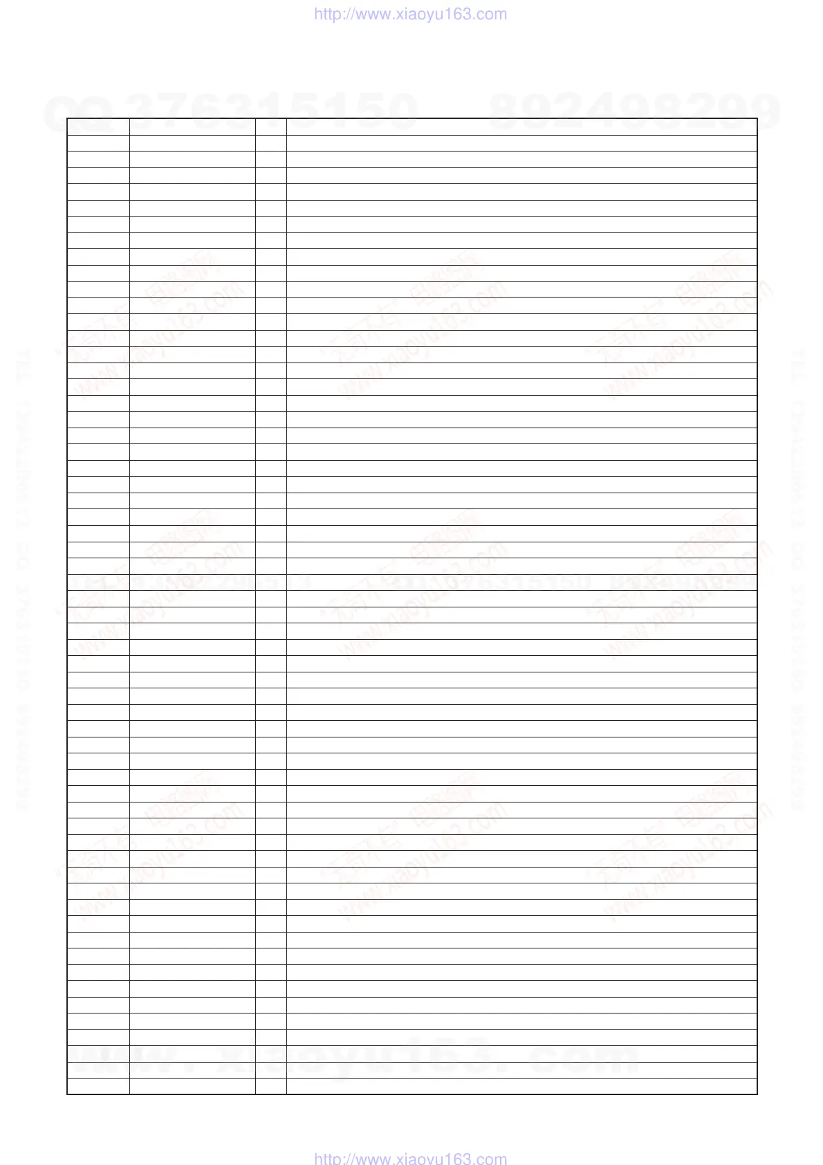
6-1
BDP-BX2/S360
SECTION 6
IC PIN FUNCTION DESCRIPTION
6-1. MAIN SYSTEM CONTROL PIN FUNCTION (MB-127 BOARD IC101: MC-10121F1-207-TA1-A)
Pin No. Name I/O Description
A1 VOID - This pin is not ball.
A2 VOID - This pin is not ball.
A3 VOID - This pin is not ball.
A4 RFN2 I RF I/F RF differential signal (-) Input
A5 RFP2 I RF I/F RF differential signal (+) Input
A6 RFN I RF I/F RF differential signal (-) Input
A7 RFP I RF I/F RF differential signal (+) Input
A8 AGND - Analog GND for Drive Controller Block
A9 E I RF I/F Main Beam Signal (E) Input
A10 F I RF I/F Main Beam Signal (F) Input
A11 D I RF I/F Main Beam Signal (D) Input
A12 A I RF I/F Main Beam Signal (A) Input
A13 CAGC1 I/O RF I/F Connection to condenser for AGC detector (normal)
A14 CAGC2 I/O RF I/F Connection to condenser for AGC detector (for CAPA)
A15 ADIN0/RFP7 I RF I/F A/D Input/GPIO 7
A16 MON1/RFP4 I/O RF I/F Internal Signal Monitor, Monitor Input Signal/GPIO 4
A17 RFEQOP O RF I/F RFEQ (+) Output (for monitor)
A18 SAGNDANA - Analog ground for Serial ATA
A19 SACREFN I Serial ATA Reference Clock Negative Input
A20 SAGNDDIG - Digital ground for Serial ATA
A21 SATXN0 O Serial ATA Serial Transmit Data0
A22 SAGNDDIG - Digital ground for Serial ATA
A23 SARXP0 I Serial ATA Serial Receive Data0
A24 SAGNDDIG - Digital ground for Serial ATA
A25 GND - Ground for digital and DDR2 SDRAM
A26 GPIO35 I/O Horizontal Sync Signal/Composite Sync Signal
A27 GND - Ground for digital and DDR2 SDRAM
A28 GPIO43 I/O VODY6: Digital Video Y Data Output
A29 GND - Ground for digital and DDR2 SDRAM
A30 N.U. I Not used (Fixed at "L")
A31 GND - Ground for digital and DDR2 SDRAM
A32 N.U. I Not used (Fixed at "H")
A33 VOID - This pin is not ball.
A34 VOID - This pin is not ball.
A35 VOID - This pin is not ball.
B1 VOID - This pin is not ball.
B2 VOID - This pin is not ball.
B3 AGND - Analog GND for Drive Controller Block
B4 AGND - Analog GND for Drive Controller Block
B5 AVDD33 - Analog 3.3V supply for Drive Controller Block
B6 CREG O RF I/F Regulator Voltage Output (1.65V)
B7 VREFIO I/O RF I/F Reference Voltage Input/Output for pickup
B8 RFTSTIN1 I RF I/F RF Test Input
B9 G/FOP I RF I/F Main Beam Signal (G) Input/FO () Input for focusing
B10 H/FOM I RF I/F Main Beam Signal (H) Input/FO () Input for focusing
B11 B I RF I/F Main Beam Signal (B) Input
B12 C I RF I/F Main Beam Signal (C) Input
B13 CEQ I/O RF I/F Connection to condenser for RF EQ fc control circuit
B14 REQ I/O RF I/F Connection to resistor for setting RF EQ circuit current
B15 ADIN1 I RF I/F A/D Input
B16 MON2/RFP5 I/O RF I/F Internal Signal Monitor, Monitor Input Signal/GPIO 5
B17 RFEQOM O RF I/F RFEQ (-) Output (for monitor)
B18 SAVDDANA - 1.8V supply (Serial ATA analog VDD)
B19 SACREFP I Serial ATA Reference Clock Positive Input
B20 SAGNDDIG - Digital ground for Serial ATA
B21 SATXP0 O Serial ATA Serial Transmit Data0
B22 SAGNDDIG - Digital ground for Serial ATA
B23 SARXN0 I Serial ATA Serial Receive Data0
B24 SAGNDDIG - Digital ground for Serial ATA
w
w
w
.
x
i
a
o
y
u
1
6
3
.
c
o
m
Q
Q
3
7
6
3
1
5
1
5
0
9
9
2
8
9
4
2
9
8
T
E
L
1
3
9
4
2
2
9
6
5
1
3
9
9
2
8
9
4
2
9
8
0
5
1
5
1
3
6
7
3
Q
Q
TEL 13942296513 QQ 376315150 892498299
TEL 13942296513 QQ 376315150 892498299
http://www.xiaoyu163.com
http://www.xiaoyu163.com