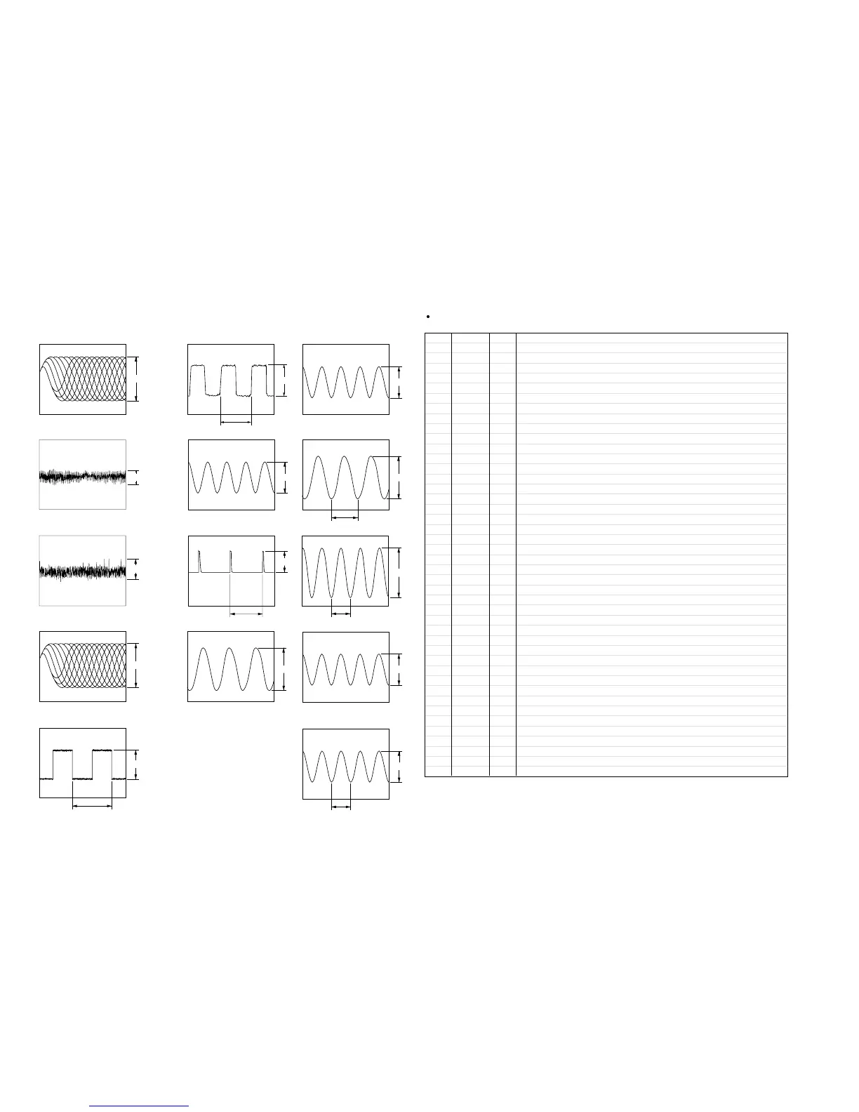
• Waveforms
– SERVO Section –
5.2 Vp-p
474 ns
2 IC101 @¶ (TE) 200 mV/DIV, 100 µs/DIV
5.2 Vp-p
16.9344 MHz
3 IC101 @ª (FE) 200 mV/DIV, 50 ns/DIV
4 IC101 #§ (RFAC) 200 mV/DIV, 500 ns/DIV
5 IC101$∞ (LRCK)
5.2 Vp-p
22.7
µ
s
4.8 Vp-p
4 MHz
1 IC101 @§ (RFDC) 200 mV/DIV, 500 ns/DIV 6 IC101 $¶ (BLCK)
7 IC101 ^™ (XTAI)
8 IC101 (§ (MDP)
9 IC201 #¡ (XTALI)
– 53 – – 54 –
840 mVp-p
45.159 MHz
1.8 Vp-p
16.9344 MHz
4 Vp-p
44 ns
1 IC602 1
– AUDIO Section –
2 IC602 6
3 IC603 0 (XIN)
4 IC604 3
5 IC610 1 (CK)
1.2 Vp-p
+0.25
–0.20
Approx. 400 mVp-p
Approx. 200 mVp-p
1.2 Vp-p
+0.25
–0.20
2.8 Vp-p
8 ns
4.8 Vp-p
180 ns
6-9. IC PIN FUNCTION DESCRIPTION
Pin No. Pin Name I/O Function
1 SRON O Sled servo drive PWM signal output terminal Not used (open)
2 SRDR O
Sled servo drive PWM signal (–) output to the BA6297AFP (IC102)
3 SFON O
Sled servo drive PWM signal output terminal Not used (open)
4 TFDR O
Tracking servo drive PWM signal (–) output to the BA6297AFP (IC102)
5 TRON O
Tracking servo drive PWM signal output terminal Not used (open)
6 TRDR O
Tracking servo drive PWM signal (+) output to the BA6297AFP (IC102)
7 TFON O
Tracking servo drive PWM signal output terminal Not used (open)
8 FFDR O
Focus servo drive PWM signal (+) output to the BA6297AFP (IC102)
9 FRON O
Focus servo drive PWM signal output terminal Not used (open)
10 FRDR O Focus servo drive PWM signal (–) output to the BA6297AFP (IC102)
11
FFON O Focus servo drive PWM signal output terminal Not used (open)
12
VCOO O Oscillator circuit output terminal for analog PLL of the playback EFM Not used (open)
13 VCOI I Oscillator circuit input terminal for analog PLL of the playback EFM Not used (fixed at “L”)
14 TEST I Input terminal for the test (fixed at “L”)
15 DVSS —
Ground terminal (digital system)
16 TES2 I Input terminal for the test (fixed at “L”)
17 TES3 I Input terminal for the test (fixed at “L”)
18 PDO O
Charge-pump output terminal for analog PLL of the playback EFM Not used (open)
19 VPCO O PLL charge-pump output terminal for the variable pitch Not used (open)
20 VCKI I Clock signal input from external VCO for the variable pitch Not used (fixed at “L”)
21
AVD2 — Power supply terminal (+5V) (analog system)
22
IGEN I Power supply terminal (+5V) (for operational amplifier)
23
AVS2 — Ground terminal (analog system)
24
ADII I Input terminal for the A/D converter Not used (open)
25
ADIO O Output terminal of the operational amplifier Not used (open)
26
RFDC I RF signal (DC level) input terminal for the digital servo process
27 TE I
Tracking error signal input from the RF amplifier in optical pick-up
28 SE I Sled error signal input from the RF amplifier in optical pick-up
29
FE I Focus error signal input from the RF amplifier in optical pick-up
30
VC I Middle point voltage (+2.5V) input from the RF amplifier in optical pick-up
31
FILO O Filter output terminal for master clock of the playback master PLL
32
FILI I Filter input terminal for master clock of the playback master PLL
33
PCO O Phase comparison output terminal for master clock of the playback EFM master PLL
34
CLTV I Internal VCO control voltage input of the playback master PLL
35
AVS1 — Ground terminal (analog system)
36
RFAC I RF signal (AC level) input terminal for the EFM demodulator
37
BIAS I Constant current input terminal of the playback EFM asymmetry circuit
38
ASYI I Playback EFM asymmetry comparator voltage input terminal
39
ASYO O Playback EFM full-swing output terminal
40 AVD1 — Power supply terminal (+5V) (analog system)
41 DVDD — Power supply terminal (+5V) (digital system)
42 ASYE I Playback EFM asymmetry circuit on/off selection input terminal (fixed at “H”)
43 PSSL I Audio data output mode selection input terminal (fixed at “L”)
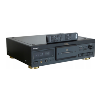
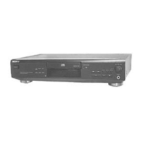
SERVO BOARD IC101 CXD2545Q
(DIGITAL SIGNAL PROCESSOR, FOCUS/TRACKING/SLED SERVO, EFM COMPARATOR)
4.8 Vp-p
22 ns