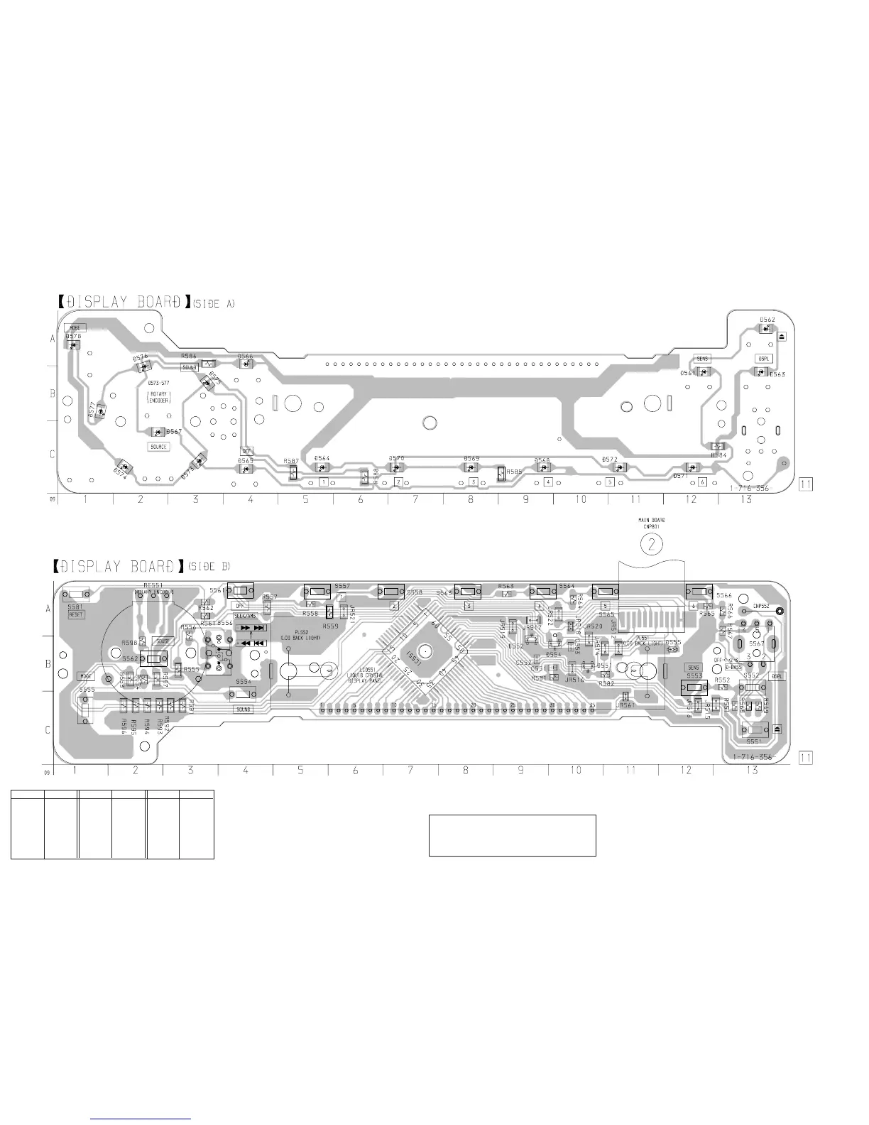
4-5. PRINTED WIRING BOARD — DISPLAY SECTION —
Note:
•
®
: Through hole.
• b : Pattern from the side which enables seeing.
(The other layer’s patterns are not indicated.)
Caution:
Pattern face side: Parts on the pattern face side seen from the
(Side B) pattern face are indicated.
Parts face side: Parts on the parts face side seen from the
(Side A) parts face are indicated.
• Semiconductor Location
Ref. No. Location
(D551) B-10
(D552) B-9
(D554) B-10
D561 B-12
D562 A-13
D563 B-13
D564 C-5
D565 C-4
Ref. No. Location
D566 A-4
D567 C-2
D568 C-9
D569 C-8
D570 C-7
D571 C-12
D572 C-11
D573 C-3
– 27 – – 28 –
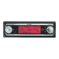
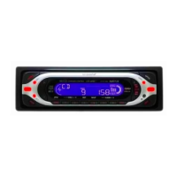
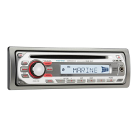
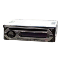
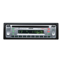
CDX-2250/3500
D574 C-2
D575 B-3
D576 A-2
D577 B-1
D578 A-1
(IC551) B-7
Ref. No. Location
( ) : SIDE B