13
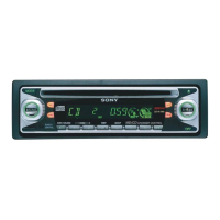
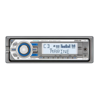
CDX-CA700/CA700X
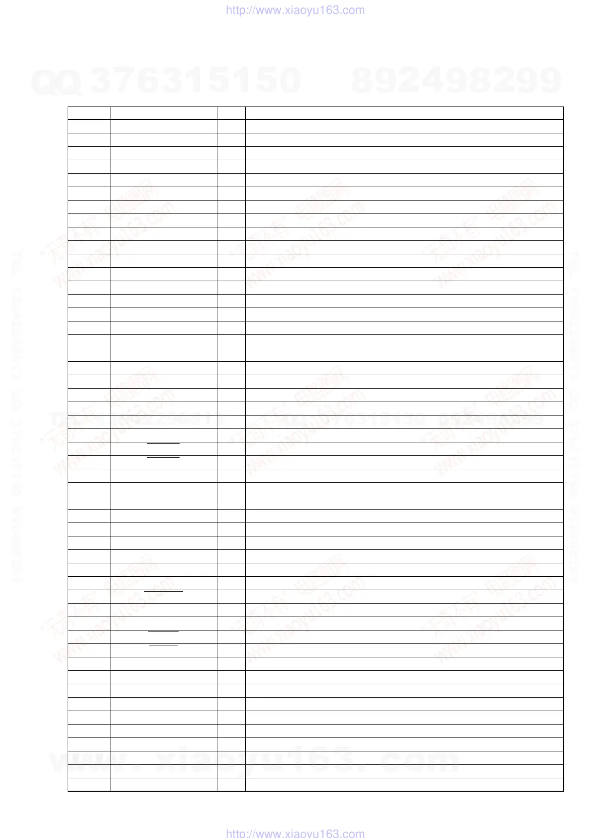
3-1. IC PIN DESCRIPTION
• IC801 MN101C49KCY2 (SYSTEM CONTROL) (US, Canadian model)
• IC801 MN101C49KCX2 (SYSTEM CONTROL) (AEP, UK model)
Pin No. Pin Name I/O Pin Description
1 VREF– — Ground for A/D converter power supply
2 VSM I S-meter voltage detection signal input from tuner unit (TU10)
3 NIL I Connect to ground.
4 KEYIN1 I Key signal input
5 KEYIN0 I Key signal input
6 RC IN0 I Rotary commander key signal input from remote in jack (J561)
7 QUALITY I Noise detection signal input
8 NIL/MPTH I Connect to ground (US, Canadian)/Multi path detection signal input (AEP, UK)
9 DSTSEL/FUNCSEL I Destination set up detection signal input
10 VREF — A/D converter power supply
11 VDD — Power supply (+5 V) input pin
12 OSCOUT O High speed clock signal output (18.432 MHz)
13 OSCIN I High speed clock signal input (18.432 MHz)
14 VSS — Ground for power supply
15 XIN I Low speed clock signal input (32.768 kHz)
16 XOUT O Low speed clock signal output (32.768 kHz)
17 MMOD I
Memory mode select signal input (Input to “Low” (single chip mode).)
(Connect to ground.)
18 LCDSO O LCD serial data signal output to LCD driver (IC901)
19 LCDCE O LCD chip enable signal output to LCD driver (IC901)
20 LCDCKO O LCD serial clock signal output to LCD driver (IC901)
21 CD TSO O CD servo IC serial data signal output
22 CD TSI I CD servo IC serial data signal input
23 CD TCKO O CD servo IC serial clock signal output
24 SYSRST O System reset signal output to bus interface (IC581)
25 BUS ON O Bus on signal output to bus interface (IC581)
26 KEYACK I Key acknowledge detection signal input
27 NIL/DAVN I
Connect to ground (US, Canadian)/RDS data block synchronization detection signal
input (AEP, UK)
28 BU IN I Back up power supply detection signal input
29 SIRCS I Remote signal input from remote control receiver (IC971)
30 CD SELFSW I CD mechanism self load position detection switch signal input from self switch (SW2)
31 CD PACK I CD text pack sync signal input from CD servo (IC1)
32 VDD2 — Power supply (+5 V) pin
33 RESET I microcomputer reset signal input from reset IC (IC551) “L”: reset
34 NOSE SW I Front panel attachment detection signal input from nose detect switch (S552) “L”: ON
35 BEEP O Beep signal output to power amp (IC751)
36 NCO O Not used. (Open)
37 TESTIN I Test mode detection signal input
38 ACCIN I Accessory power supply detection signal input
39 NCO (VCC) O Not used. (Open)
40 TELATT I Telephone ATT detection signal input
41 NCO (VCC) I Connect to power supply.
42 UNISO O Sony-Bus serial data signal output to bus interface (IC581)
43 UNISI I Sony-Bus serial data signal input from bus interface (IC581)
44 UNICKO O Sony-Bus serial clock signal output to bus interface (IC581)
45 I2C SIO I/O I2C bus serial data signal input/output
46 NCO O Not used. (Open)
47 I2C CKO O I2C bus serial clock signal output
48 NCO O Not used. (Open)
SECTION 3
DIAGRAMS
Ver 1.1
w
w
w
.
x
i
a
o
y
u
1
6
3
.
c
o
m
Q
Q
3
7
6
3
1
5
1
5
0
9
9
2
8
9
4
2
9
8
T
E
L
1
3
9
4
2
2
9
6
5
1
3
9
9
2
8
9
4
2
9
8
0
5
1
5
1
3
6
7
3
Q
Q
TEL 13942296513 QQ 376315150 892498299
TEL 13942296513 QQ 376315150 892498299
http://www.xiaoyu163.com
http://www.xiaoyu163.com