70
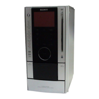
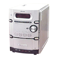
HCD-AZ2D/AZ5D
Pin No. Pin Name I/O Description
187 MSW O DVD/CD selection signal output terminal
188 DSEL O Interlace/progressive selection signal output to the video amplifier
189 DAVCC – Power supply terminal (+3.3V)
190 VREF – For bandgap reference voltage terminal
191 FS – Full scale adjustment terminal
192 YUV0 O Video data output terminal Not used
193 DAVSS – Ground terminal
194 YUV1 O Y signal output to the video amplifier
195 DAVDD – Power supply terminal (+3.3V)
196 YUV2 O Chroma signal output to the video amplifier
197 DAVSS – Ground terminal
198 YUV3 O Video signal output to the video amplifier
199 DAVDD – Power supply terminal (+3.3V)
200 YUV4 O Chroma signal output to the video amplifier
201 DAVSS – Ground terminal
202, 203 YUV5, YUV6 O Component video signal output to the video amplifier
204 DVDD3 – Power supply terminal (+3.3V)
205 MIC I Microphone detection signal input terminal “H”: microphone in
206 VOICE – Not used
207 KRMOD O Karaoke mode selection signal output to the system controller
208 SMSCK – Not used
209 SPDATA I SPDIF digital audio data input from the A/D converter (HCD-AZ5D only)
210 SMSDO – Not used
211 XSMCS – Not used
212 DVDD3 – Power supply terminal (+3.3V)
213 ALRCK O L/R sampling clock signal output to the D/A converter and A/D converter
214 ABCK O Bit clock signal output to the D/A converter and A/D converter
215 ACLK O Master clock signal output to the D/A converter and A/D converter
216 DVSS – Ground terminal
217 to 219 ASDATA0 to ASDATA2 O Audio serial data output to the D/A converter
220 XRST O Reset signal output to the D/A converter “L”: reset
221 DVDD18 – Power supply terminal (+1.8V)
222 ASDATA4 O Audio serial data output to the D/A converter
223 DVSS – Ground terminal
224 DWIDE – Not used
225 SPDIF O SPDIF digital audio signal output terminal (HCD-AZ2D only)
226 RFGND18 – Ground terminal
227 RFVDD18 – Power supply terminal (+1.8V)
228 XTALO O System clock output terminal (27 MHz)
229 XTALI I System clock input terminal (27 MHz)
230 JITFO O Output terminal of the RF jitter meter
231 JITFN I Input terminal of the RF jitter meter
232 PLLVSS – Ground terminal
233 IDAC – Not used
234 PLLVDD3 – Power supply terminal (+3.3V)
235 LPFON O Data PLL loop filter output terminal
236 LPFIP I Data PLL loop filter input terminal
237 LPFIN I Data PLL loop filter input terminal
238 LPFOP O Data PLL loop filter output terminal
239 VDD3 – Power supply terminal (+3.3V)
w
w
w
.
x
i
a
o
y
u
1
6
3
.
c
o
m
Q
Q
3
7
6
3
1
5
1
5
0
9
9
2
8
9
4
2
9
8
T
E
L
1
3
9
4
2
2
9
6
5
1
3
9
9
2
8
9
4
2
9
8
0
5
1
5
1
3
6
7
3
Q
Q
TEL 13942296513 QQ 376315150 892498299
TEL 13942296513 QQ 376315150 892498299
http://www.xiaoyu163.com
http://www.xiaoyu163.com