
D
Douglas ValentineJul 29, 2025
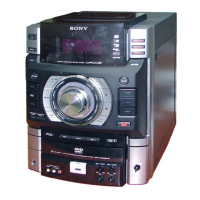
What to do if the optical pickup has a problem on Sony HCD-GT3D?
- JJennifer JohnsonJul 29, 2025
If the optical pickup in your Sony Receiver is malfunctioning, the suggested solution is to replace the BU.
What to do if the optical pickup has a problem on Sony HCD-GT3D?
If the optical pickup in your Sony Receiver is malfunctioning, the suggested solution is to replace the BU.
Details the specifications for the FM tuner, including tuning range and antenna type.
Outlines BLUETOOTH specifications, communication system, and supported profiles/codecs.
Details methods and limits for measuring AC leakage current from exposed metal parts.
Characteristics of unleaded solder and precautions for its use during repairs.
Precautions for handling the optical pick-up block to prevent electrostatic breakdown.
Outlines the sequence of disassembly steps for the entire unit.
Details the procedure for removing the left and right side panels.
Information on identifying the model number and destination code via the rear label.
Step-by-step guide for pairing Bluetooth devices with the system.
Notes on using specified bond for fixing replaced parts, especially on the DAMP board.
Procedure for manually opening the disc tray when the unit is powered off.
Safety procedure for discharging capacitors on the SMPS board before servicing.
Details the procedure for removing the left and right side panels.
Explains how to remove the top panel section of the unit.
Instructions for removing the optical board assembly.
Steps for removing the loading panel assembly.
Procedure for removing the CDM (Compact Disc Mechanism) section.
Steps for removing the back panel of the unit.
Guide for removing the DAMP board.
Instructions for removing the main MOTHERBOARD and SPLITTER boards.
Steps for removing the sub chassis assembly.
Procedure for removing the SMPS (Switch Mode Power Supply) board.
Steps for removing the main chassis of the unit.
Guide for removing the front panel assembly.
Instructions for removing the loudspeaker unit.
Clears all data, including history, for returning the set to the customer.
Enters a diagnostic mode for easy diagnosis and adjustment using the TV.
Procedure for executing IOP measurement as part of the diagnostic process.
Method for checking the focus bias using an oscilloscope and test disc.
A diagnostic flowchart for troubleshooting the SMPS board power outputs.
Troubleshooting flowchart for the optical block, starting with pickup movement.
Continues the optical block diagnosis, checking laser diode and RF signal levels.
Diagnostic flow for checking audio output and voltages from the DAMP board.
Illustrates the physical locations of various circuit boards within the unit.
Block diagram showing the signal flow for servo, USB, and display functions.
Block diagram illustrating the audio and video signal paths.
Block diagram detailing the audio amplifier section's signal flow.
Block diagram showing the power supply distribution and control.
Displays key waveforms for various ICs on the MOTHERBOARD board.
Shows the component and conductor sides of the MOTHERBOARD printed wiring board.
First part of the schematic diagram for the MOTHERBOARD board.
Second part of the schematic diagram for the MOTHERBOARD board.
Third part of the schematic diagram for the MOTHERBOARD board.
Fourth part of the schematic diagram for the MOTHERBOARD board.
Fifth part of the schematic diagram for the MOTHERBOARD board.
Sixth part of the schematic diagram for the MOTHERBOARD board.
Seventh part of the schematic diagram for the MOTHERBOARD board.
Eighth part of the schematic diagram for the MOTHERBOARD board.
Ninth part of the schematic diagram for the MOTHERBOARD board.
Tenth and final part of the schematic diagram for the MOTHERBOARD board.
Shows the component and conductor sides of the DAMP board's printed wiring.
First part of the schematic diagram for the DAMP board.
Second part of the schematic diagram for the DAMP board.
Shows the printed wiring board layout for the BUTTON board.
Schematic diagram for the BUTTON board, detailing its components and connections.
Shows the printed wiring board layout for the LCD module.
Printed wiring board layout for the OPTICAL board.
Printed wiring board layout for the SPK_HLED board.
Printed wiring board layout for the MIC board.
Schematic diagram for the MIC board, showing its circuitry and connections.
Printed wiring board layout for the SPLITTER board.
Block diagram for IC1001, detailing its input/output and internal functions.
Block diagram for IC106, a 32M-bit Serial Flash Memory.
Block diagram for IC401, handling optical pickup control and signals.
Block diagram for IC502, a LED driver with PWM output.
Block diagram for IC606, stereo ADCs with digital filters.
Block diagram for IC902, a radio tuner IC.
Block diagram for IC914, a stereo DAC with digital filter.
Pin function descriptions for IC101, the system controller.
Pin function descriptions for IC301, the CD RF AMP and servo processor.
Exploded view showing the parts of the side panel assembly.
Exploded view showing the parts of the top panel assembly.
Exploded view showing the parts of the loading panel assembly.
Exploded view showing the MOTHERBOARD board and related parts.
Exploded view showing the main chassis and its components.
Exploded view showing the parts of the front panel assembly.
Exploded view showing the parts of the CD mechanism section.
Exploded view of the CD mechanism assembly with part numbers.
Parts list for the BUTTON board, including resistors, capacitors, connectors, and switches.
Parts list for the DAMP board, including capacitors, ICs, transistors, and resistors.
Parts list for the MIC board, including resistors, capacitors, diodes, and connectors.
Parts list for the MOTHERBOARD board, covering capacitors and ICs.
Continues the parts list for the MOTHERBOARD board, detailing capacitors.
Continues the parts list for the MOTHERBOARD board, detailing capacitors.
Continues the parts list for the MOTHERBOARD board, detailing capacitors, diodes, ferrite beads, filters, and ICs.
Continues the parts list for the MOTHERBOARD board, detailing ICs and connectors.
Continues the parts list for the MOTHERBOARD board, detailing jacks, jumpers, coils, transistors, and resistors.
Continues the parts list for the MOTHERBOARD board, detailing resistors.
Continues the parts list for the MOTHERBOARD board, detailing resistors.
Continues the parts list for the MOTHERBOARD board, detailing resistors.
Continues the parts list for the MOTHERBOARD board, detailing resistors, composition circuit blocks, thermistors, and vibrators.
Parts list for the MS-476 board, including capacitors, ICs, jumpers, resistors, connectors, and diodes.
Parts list for the OPTICAL board, including capacitors and ICs.
Parts list for the SPLITTER board, including connectors and resistors.
| Speaker Configuration | 2.1 Channel |
|---|---|
| CD Player | Yes |
| Supported Disc Formats | CD, CD-R/RW |
| DVD Playback | No |
| FM Tuner | Yes |
| AM Tuner | Yes |
| Bluetooth | Yes |
| USB Playback | Yes |
| NFC | Yes |
| Bass Boost Function | Yes |
| Remote Control | Yes |
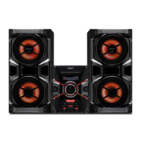
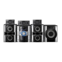
| Type | Mini Hi-Fi System |
| Preset Stations | 30 |
| USB Port | Yes |
| Audio In | Yes (Analog) |
| Equalizer | Yes |