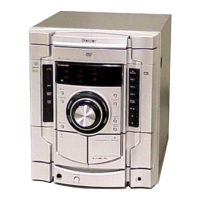
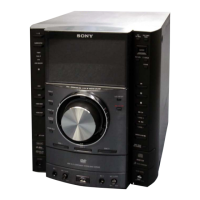
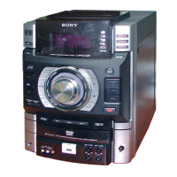
HCD-GT3D
HCD-GT3D
3737
Note on Schematic Diagram:
• All capacitors are in μF unless otherwise noted. (p: pF)
50 WV or less are not indicated except for electrolytics
and tantalums.
• All resistors are in Ω and
1
/4 W or less unless otherwise
specifi ed.
• Components for right channel have same values as for
left channel. Reference numbers are coded from
• C : panel designation.
• Note for Printed Wiring Boards and Schematic Diagrams
• A : B+ Line.
• Voltage and waveforms are dc with respect to ground
under no-signal (detuned) conditions.
no mark : TUNER
• Voltages are taken with a VOM (Input impedance 10 MΩ).
Voltage variations may be noted due to normal production
tolerances.
• Waveforms are taken with a oscilloscope.
Voltage variations may be noted due to normal production
tolerances.
• Circled numbers refer to waveforms.
• Signal path.
c : CD/DVD PLAY
f : TUNER
N : MIC
F : AUDIO (ANALOG)
L : AUDIO (DIGITAL)
E : VIDEO
d : USB
• Abbreviation
AR : Argentina model
AUS : Australian model
E4 : African model
EA : Saudi Arabia model
LA9 : Latin-American model
MY : Malaysia model
RU : Russian model
TH : Thai model
Note on Printed Wiring Board:
• X : parts extracted from the component side.
• Y : Parts extracted from the conductor side.
•
: Pattern from the side which enables seeing.
(The other layer’s patterns are not indicated.)
Caution:
Pattern face side:
(Conductor Side)
Parts face side:
(Component Side)
Parts on the pattern face side seen
from the pattern face are indicated.
Parts on the parts face side seen from
the parts face are indicated.
Note: The components identifi ed by mark 0 or dotted line
with mark 0 are critical for safety.
Replace only with part number specifi ed.
• Abbreviation
AR : Argentina model
AUS : Australian model
E4 : African model
EA : Saudi Arabia model
LA9 : Latin-American model
MY : Malaysia model
RU : Russian model
TH : Thai model
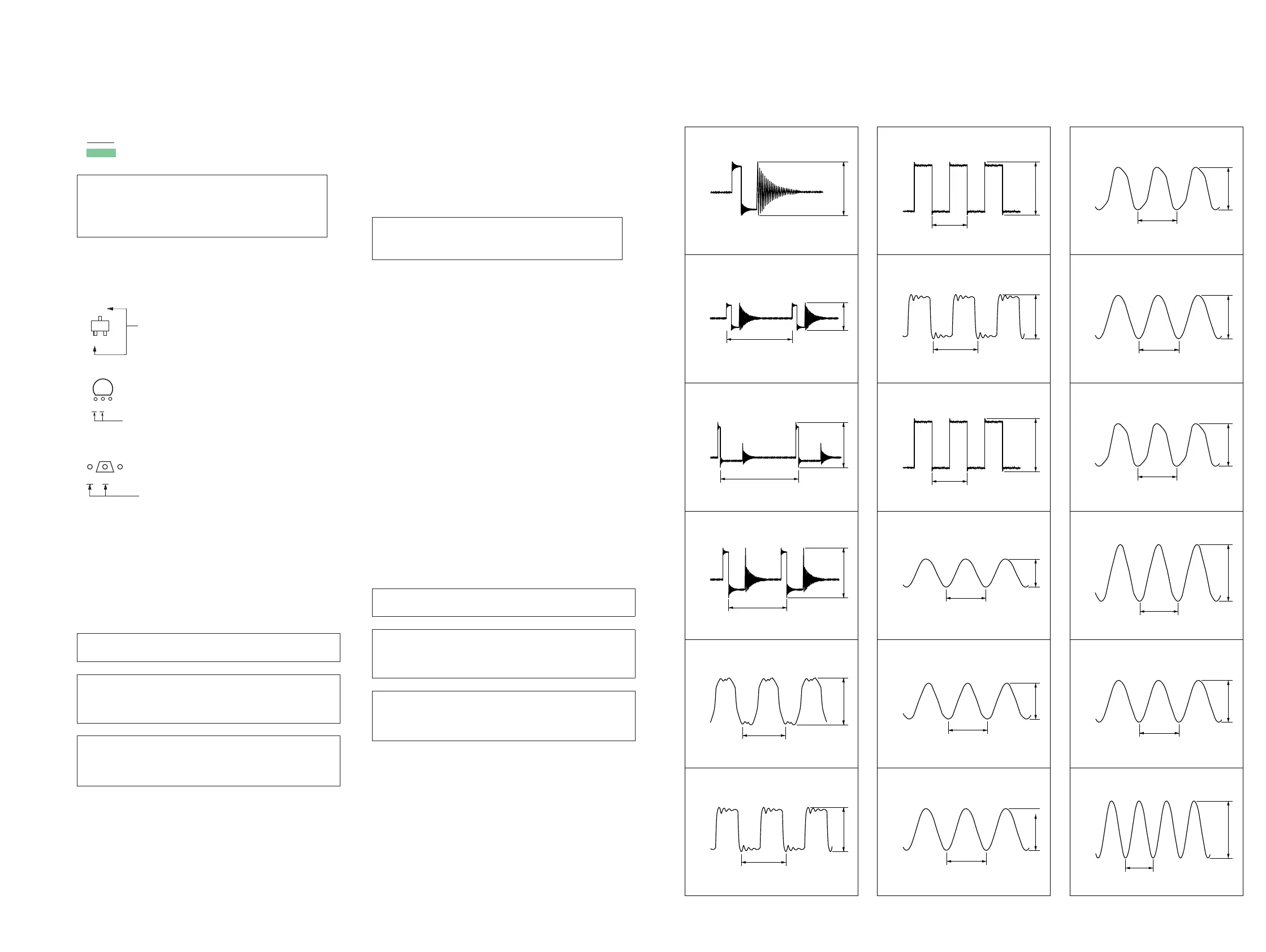
• Waveforms
- MOTHERBOARD Board -
• Indication of transistor.
C
B
These are omitted.
E
Q
CEB
These are omitted.
B
These are omitted.
CE
Q
• MOTHERBOARD board is multi-layer board.
However, the patterns of intermediate layers have not
been included in diagrams.
1 IC001 2 (VBST1)
5 V/DIV, 1 Ps/DIV
15 Vp-p
2 IC001 qg (VBST2)
5 V/DIV, 1 Ps/DIV
7.4 Ps
23 Ps
5.5 Ps
3.8 Ps
81 ns
355 ns
16 Vp-p
16 Vp-p
3 IC002 2 (VBST1)
5 V/DIV, 1 Ps/DIV
4 IC002 qg (VBST2)
5 V/DIV, 1 Ps/DIV
5 IC101 qf (AUDIO_CLK_OUT)
1 V/DIV, 25 ns/DIV
6 IC101 wf (SSI3_BCKO)
1 V/DIV, 100 ns/DIV
7 IC101 wh (SSI3_LRCKO)
1 V/DIV, 10 Ps/DIV
8 IC101 wl (SSI0_BCKO)
1 V/DIV, 100 ns/DIV
9 IC101 e; (SSI0_LRCKO)
1 V/DIV, 10 Ps/DIV
q; IC101 yj (RTC-X1)
500 mV/DIV, 10 Ps/DIV
qa IC101 yk (RTC-X2)
500 mV/DIV, 10 Ps/DIV
qs IC101 u; (EXTAL)
500 mV/DIV, 25 ns/DIV
qd IC101 ua (XTAL)
1 V/DIV, 25 ns/DIV
qf IC101 oa (AUDIO-X1)
500 mV/DIV, 25 ns/DIV
qg IC101 os (AUDIO-X2)
1 V/DIV, 25 ns/DIV
qh IC101 <zc. (USB-X1)
200 mV/DIV, 10 ns/DIV
qj IC101 <zv/ (USB-X2)
200 mV/DIV, 10 ns/DIV
qk IC301 7 (XTALI)
200 mV/DIV, 25 ns/DIV
3.7 Vp-p
75 ns
3.4 Vp-p
81 ns
3.4 Vp-p
21 ns
630 mVp-p
81 ns
1.7 Vp-p
21 Ps
30 Ps
30 Ps
75 ns
3.5 Vp-p
1 Vp-p
1.6 Vp-p
1.7 Vp-p
21 ns
37.5 ns
480 mVp-p
640 mVp-p
3.6 Vp-p
3.6 Vp-p
325 ns
3.56 Vp-p
16 Vp-p
Note 1: When the MS-476 board is defective, exchange the
entire LOADING COMPLETE ASSY (T).
Note 1: When the MS-476 board is defective, exchange the
entire LOADING COMPLETE ASSY (T).
Note 3: When the C1126, C1127, C1128, C1129, C1142,
L1010 and RY001 on the DAMP board are replaced,
spread the bond referring to “BOND FIXATION OF
ELECTRIC PARTS” on servicing notes (page 6).
Note 3: When the C1126, C1127, C1128, C1129, C1142,
L1010 and RY001 on the DAMP board are replaced,
spread the bond referring to “BOND FIXATION OF
ELECTRIC PARTS” on servicing notes (page 6).
Note 2: When the complete DAMP board is replaced, refer to
“NOTE OF REPLACING THE IC1001 ON THE DAMP
BOARD AND THE COMPLETE DAMP BOARD” on
servicing notes (page 5).
Note 2: When the complete DAMP board is replaced, refer to
“NOTE OF REPLACING THE IC1001 ON THE DAMP
BOARD AND THE COMPLETE DAMP BOARD” on
servicing notes (page 5).
Ver. 1.1