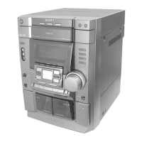
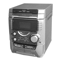
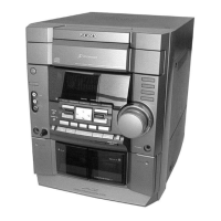
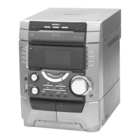
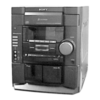
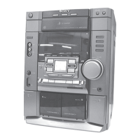
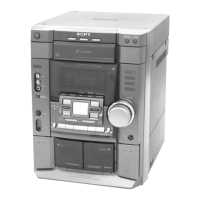
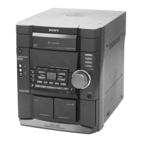
HCD-DX70
4444
6-24. IC PIN FUNCTIONS
1 SOSQ O Sub-Q serial output.
2 SQCK I Clock input for SQSO read-out
3 XRST I System reset.
4 SYSM I Muting input.
5 DATA I Serial date input,supplied from CPU.
6 XLAT I Latch input,supplied from CPU.
7 CLOK I Serial date transfer clock input,supplied from CPU.
8 SENS O SENS output.
9 SCLK I SENS serial data read-out clock.
10 VDD — Power supply.
11 ATSK I/O Input pin for anti-shock (Ground)
12 SPOA I Ground.
13 SPOB I Ground.
14 XLON O Not used.
15 WFON O Not used.
16 XUGF O Not used.
17 XPCK O Not used.
18 GFS O Not used.
19 2SPO O Not used.
20 SCOR O Sub-code sync output.
21 COUT I/O Not used.
22 MIRR I/O Not used.
23 DFCT I/O Not used.
24 FOK I/O Not used.
25 LOCK I/O Not used.
26 MDP O Output to control spindle motor servo.
27 SSTP I Input signal to detect disc inner most trak.
28 SFDR O Sled drive output.
29 SRDR O Sled drive output.
30 TFDR O Tracking drive output.
31 TRDR O Tracking drive output.
32 FFDR O Focus drive output.
33 FRDR O Focus drive output.
34 VSS — Ground.
35 TEST I TEST pin connected normally ground.
36 TES1 I TEST pin connected normally ground.
37 XTSL I X’tal selection circuit input.
38 VC I Center voltage input.
39 FE I FOCUS error signal input.
40 SE I Sled error signal input.
41 TE I Tracking error signal input.
42 CE I Center servo analog input.
43 RFDC I RF signal input.
44 ADIO O Not used.
45 AVSS0 — Analog ground.
46 IGEN I Power supply pin operational amplifiers.
47 AVDDO — Analog power supply.
48 ASYO O EFM full swing output.
49 ASYI I Asymmetry comparator voltage input.
50 BIAS I Asymmetry circuit constant current input.
51 RFAC I EFM signal input.
52 AVSS3 — Analog ground.
FunctionPin NamePin No. I/O
• IC101 DIGITAL SIGNAL PROCESSOR (CXD3017Q) (BD Board)
53 CLTV I Control voltage input for master VCO.
54 FILO O Filter output for master PLL.
55 FILI I Filter input for master PLL.
56 PCO O Chage-pump output for master PLL.
57 AVDD3 — Analog powr supply.
58 VSS — Ground.
59 VDD — Power supply.
60 DOUT O Not used.
61 LRCK O Not used.
62 PCMD O Not used.
63 BCK O Not used.
64 EMPH O Not used.
65 XVDD — Master clock power supply.
66 XTAI I X’tal oscillator circuit input.
67 XTAO O X’tal oscillator circuit output.
68 XVSS — Master clock ground.
69 AVDD1 — Analog power supply.
70 AOUT1 O Lch: Analog output.
71 AIN1 I Lch: OPAMP input.
72 LOUT1 O Lch: LINE output
73 AVSS1 — Analog ground.
74 AVSS2 — Analog ground.
75 LOUT2 O Rch: LINE output.
76 AIN2 I Rch: OPAMP input.
77 AOUT2 O Rch: Analog output.
78 AVDD2 — Analog power supply.
79 RMUT O Not used.
80 LMUT O Not used.
FunctionPin NamePin No. I/O
 Loading...