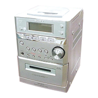
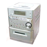
1616
HCD-EP313
SECTION 6
DIAGRAMS
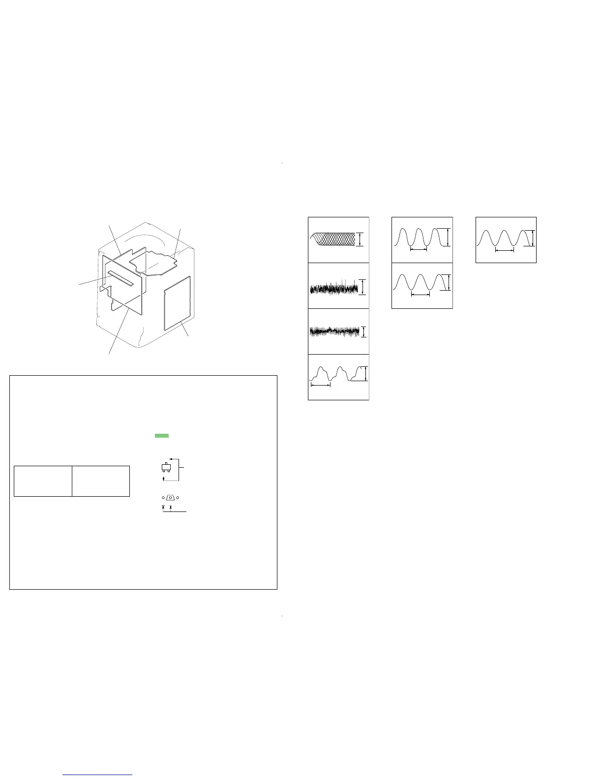
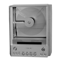
• Circuit Boards Location
THIS NOTE IS COMMON FOR PRINTED WIRING
BOARDS AND SCHEMATIC DIAGRAMS.
(In addition to this, the necessary note is printed
in each block.)
For schematic diagrams.
Note:
• All capacitors are in µF unless otherwise noted. pF: µµF
50 WV or less are not indicated except for electrolytics
and tantalums.
• All resistors are in Ω and
1
/
4
W or less unless otherwise
specified.
•
f
: internal component.
• 2 : nonflammable resistor.
• 1 : fusible resistor.
• C : panel designation.
For printed wiring boards.
Note:
• X : parts extracted from the component side.
• Y : parts extracted from the conductor side.
•
f
: internal component.
• : Pattern from the side which enables seeing.
• A : B+ Line.
• B : B– Line.
•Voltages are taken with a VOM (Input impedance 10 MΩ).
Voltage variations may be noted due to normal produc-
tion tolerances.
•Waveforms are taken with a oscilloscope.
Voltage variations may be noted due to normal produc-
tion tolerances.
• Circled numbers refer to waveforms.
•Abbreviation
CND : Canadian model
• Signal path.
F : TUNER (FM)
J : CD
d : MD
E : PB (TAPE)
a : REC (TAPE)
•Waveforms
– CD Board –
6
IC301 7 32kHz OUT
1V/DIV,
10
µ
s
/DIV
5V/DIV,
10 ms
/DIV
5
IC301 0 8.6MHz OUT
10Vp-p
20
m
s
2.4Vp-p
30
µ
s
7 Q453,Q454
collector
(Rec mode)
5V/DIV,
5
µ
s
/DIV
10Vp-p
10
µ
s
– CONTROL Board – – MAIN Board –
Note:
The components identified by
mark 0 or dotted line with mark
0 are critical for safety.
Replace only with part number
specified.
Note:
Les composants identifiés par
une marque 0 sont critiques
pour la sécurité.
Ne les remplacer que par une
pièce portant le numéro spécifié.
• Indication of transistor
C
B
These are omitted.
E
Q
B
These are omitted.
CE
MAIN board
CONTROL board
BACK LIGHT board
TRANSFORMER board
CD board