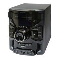
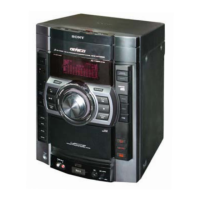
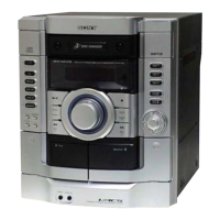
HCD-GX470/GX570
2727
HCD-GX470/GX570
• Note For Printed Wiring Boards and Schematic Diagrams
• Indication of transistor
Note on Schematic Diagram:
• All capacitors are in µF unless otherwise noted. (p: pF)
50 WV or less are not indicated except for electrolytics
and tantalums.
• All resistors are in Ω and
1
/
4
W or less unless otherwise
specified.
• f : internal component.
• 2 : nonflammable resistor.
• 5 : fusible resistor.
• C : panel designation.
• A : B+ Line.
• B : B– Line.
• Voltages and waveforms are dc with respect to ground
under no-signal (detuned) conditions.
– CD Board –
no mark :CD PLAY
– XM Board –
no mark : XM
– Other Boards –
no mark : TUNER (FM/AM)
(): CD PLAY
〈〈 〉〉 : TAPE PLAY
{ }: TAPE REC
[]: XM
∗ : Impossible to measure
• Voltages are taken with a VOM (Input impedance 10 MΩ).
Voltage variations may be noted due to normal produc-
tion tolerances.
• Waveforms are taken with a oscilloscope.
Voltage variations may be noted due to normal produc-
tion tolerances.
• Circled numbers refer to waveforms.
• Signal path.
F : TUNER (FM/AM)
J : CD PLAY
E : TAPE PLAY (DECK-A)
d : TAPE PLAY (DECK-B)
G : REC
O : XM
f : AUDIO IN
Note on Printed Wiring Board:
• X : parts extracted from the component side.
• Y : parts extracted from the conductor side.
• f : internal component.
•
: Pattern from the side which enables seeing.
(The other layers' patterns are not indicated.)
Caution:
Pattern face side: Parts on the pattern face side seen from
(Conductor Side) the pattern face are indicated.
Parts face side: Parts on the parts face side seen from
(Component Side) the parts face are indicated.
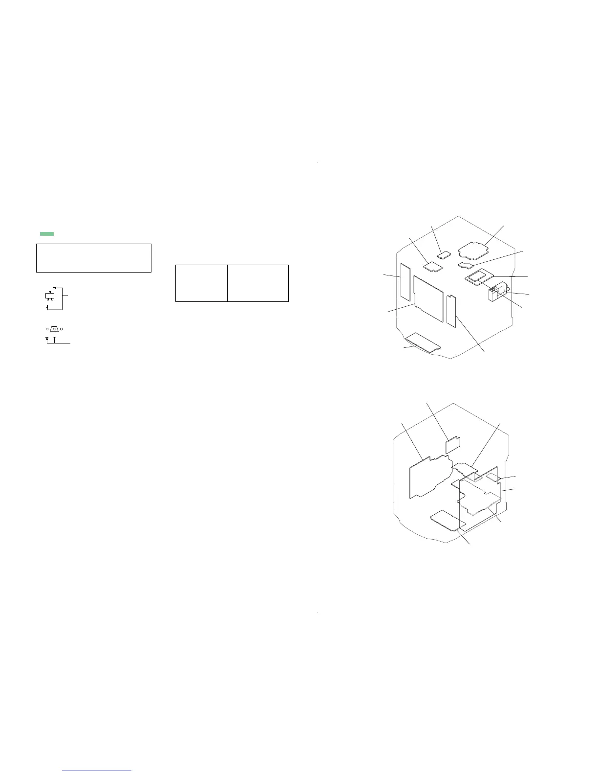
• Circuit Boards Location
C
B
These are omitted.
E
Q
B
These are omitted.
CE
Q
CD board
SW board
MOTOR (LD) board
SENSOR board
DRIVER board
MOTOR (TB) board
TUNER (FM/AM