2
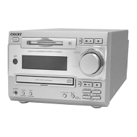
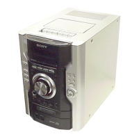
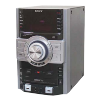
HCD-GX470/GX570
2. DIAGRAMS
• Note for Printed Wiring Boards and Schematic Diagrams
Note on Schematic Diagram:
• All capacitors are in µF unless otherwise noted. (p: pF)
50 WV or less are not indicated except for electrolytics
and tantalums.
• All resistors are in Ω and
1
/
4
W or less unless otherwise
specified.
Note on Printed Wiring Board:
• X : parts extracted from the component side.
• Y : parts extracted from the conductor side.
• : Pattern from the side which enables seeing.
(The other layers' patterns are not indicated.)
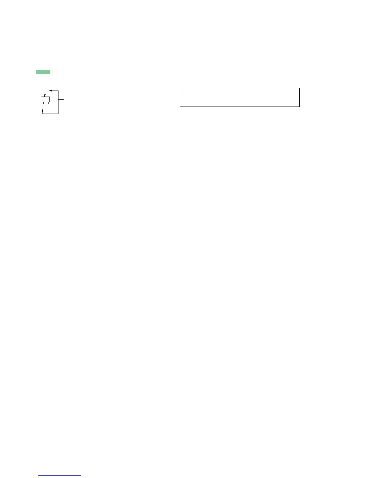
• Indication of transistor
• A : B+ Line.
• Voltages and waveforms are dc with respect to ground
under no-signal (detuned) conditions.
〈〈 〉〉 : TAPE PLAY
{ }: REC
• Voltages are taken with a VOM (Input impedance 10 MΩ).
Voltage variations may be noted due to normal produc-
tion tolerances.
• Signal path.
E : TAPE PLAY (DECK-A)
d : TAPE PLAY (DECK-B)
G : REC
C
B
These are omitted.
E
Q
Note: The components identified by mark 0 or dotted line
with mark 0 are critical for safety.
Replace only with part number specified.