SERVICE MANUAL
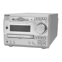
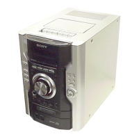
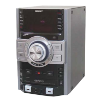
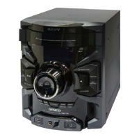
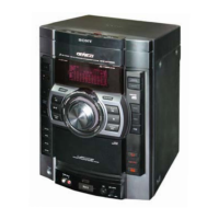
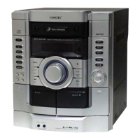
HCD-GX470/570
1
HCD-GX470/GX570
9-887-123-82
Ver. 1.2 2006.06
Subject: Change of MAIN and KEY RIGHT boards
(Suffix-13)
US Model
Canadian Model
HCD-GX470/GX570
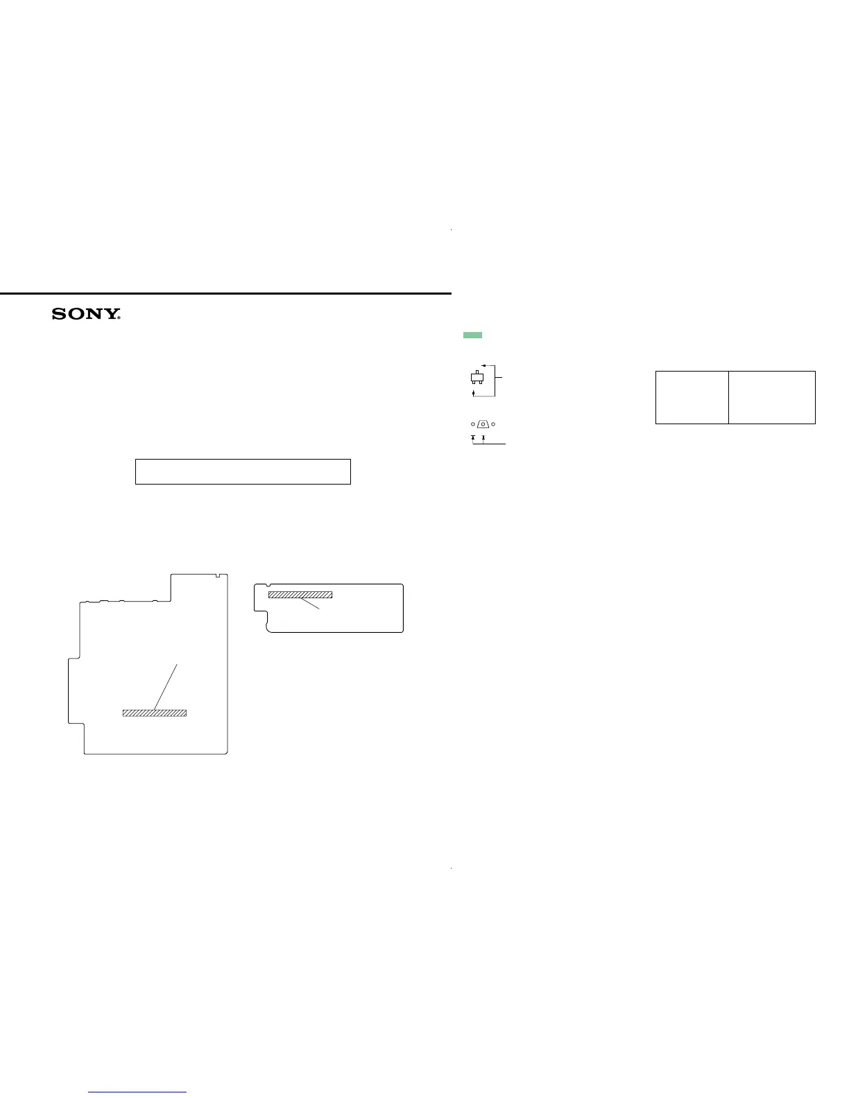
1. NEW/FORMER DESCRIPTION
In this set, MAIN and KEY RIGHT boards have been changed in the midway
of production.
Printed wiring board and schematic diagram of new type, and changed parts
list are described in this supplement-2.
Refer to original service manual and supplement-1 for other information.
– MAIN Board (Component Side) –
– KEY RIGHT Board (Component Side) –
Former : 1-869-003-12
New : 1-869-003-13
Former : 1-869-007-12
New : 1-869-007-13
SUPPLEMENT-2
File this supplement with the service manual.
2. DIAGRAMS
• Note for Printed Wiring Boards and Schematic Diagrams
• Indication of transistor
Note on Schematic Diagram:
• All capacitors are in µF unless otherwise noted. (p: pF)
50 WV or less are not indicated except for electrolytics
and tantalums.
• All resistors are in Ω and
1
/
4
W or less unless otherwise
specified.
• f : internal component.
• 2 : nonflammable resistor.
• C : panel designation.
• A : B+ Line.
• B : B– Line.
• Voltages are dc with respect to ground under no-signal
(detuned) conditions.
no mark : TUNER (FM/AM)
(): CD PLAY
〈〈 〉〉 : TAPE PLAY
{ }: TAPE REC
[]: XM
• Voltages are taken with a VOM (Input impedance 10 MΩ).
Voltage variations may be noted due to normal produc-
tion tolerances.
• Signal path.
F : TUNER (FM/AM)
J : CD PLAY
E : TAPE PLAY
G : REC
O : XM
f : AUDIO IN
Note on Printed Wiring Board:
• X : parts extracted from the component side.
• Y : parts extracted from the conductor side.
• f : internal component.
• : Pattern from the side which enables seeing.
(The other layers' patterns are not indicated.)
C
B
These are omitted.
E
Q