99
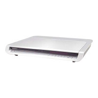
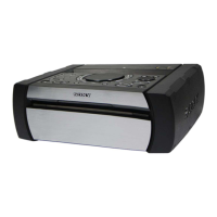
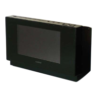
HCD-SR1/SR2/SR3
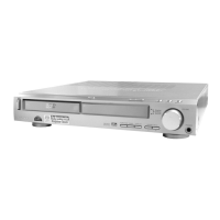
HCD-SR1/SR2/SR3
For Schematic Diagrams.
Note:
• All capacitors are in µF unless otherwise noted. (p: pF)
50 WV or less are not indicated except for electrolytics and
tantalums.
• All resistors are in Ω and
1
/
4
W or less unless otherwise
specified.
• f : internal component.
• C : panel designation.
• A : B+ Line.
• B : B– Line.
• Voltages and waveforms are dc with respect to ground un-
der no-signal (detuned) conditions.
• Voltages and waveforms are dc with respect to ground in
service mode.
• Waveforms are taken with a oscilloscope.
Voltage variations may be noted due to normal production
tolerances.
no mark : DVD STOP
• Circled numbers refer to waveforms.
• Signal path.
F : AUDIO
J : CD PLAY
c : DVD PLAY
d : TUNER
L : VIDEO
i : OPTICAL DIGITAL IN
h : VIDEO IN
a : CHROMA
E : Y
r : COMPONENT VIDEO
e : AUX IN
I : SACD PLAY
q : R, G, B
• Abbreviation
AUS : Australian model
HK : Hong Kong model
KR : Korean model
MX : Mexican model
RU : Russian model
SP : Singapore model
For Printed Wiring Boards.
Note:
• X : parts extracted from the component side.
• a : Through hole.
• : Pattern from the side which enables seeing.
(The other layers' patterns are not indicated.)
• Indication of transistor
THIS NOTE IS COMMON FOR PRINTED WIRING BOARDS AND SCHEMATIC DIAGRAMS.
(In addition to this, the necessary note is printed in each block.)
Caution:
Pattern face side: Parts on the pattern face side seen from
(Side A) the pattern face are indicated.
Parts face side: Parts on the parts face side seen from
(Side B) the parts face are indicated.
Note: The components identified by mark 0 or dotted line
with mark 0 are critical for safety.
Replace only with part number specified.
CEB
These are omitte
Q
C
EB
These are omitte
MEMO
w
w
w
.
x
i
a
o
y
u
1
6
3
.
c
o
m
Q
Q
3
7
6
3
1
5
1
5
0
9
9
2
8
9
4
2
9
8
T
E
L
1
3
9
4
2
2
9
6
5
1
3
9
9
2
8
9
4
2
9
8
0
5
1
5
1
3
6
7
3
Q
Q
TEL 13942296513 QQ 376315150 892498299
TEL 13942296513 QQ 376315150 892498299
http://www.xiaoyu163.com
http://www.xiaoyu163.com