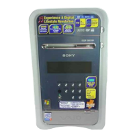
HCD-SH2000
61
• IC Pin Function Descriptions
MAIN BOARD (1/4) IC100 R5F3650KBDFA (SYSTEM CONTROL)
Pin No. Pin Name I/O Description
1 FL-DATA O Serial data output signal to FL Driver, PT6324
2 FL-CLK O Serial data clock signal to FL Driver, PT6324
3 LED-DRIVER-LATCH O Latch Signal to LED Driver, R8A66166SP
4 SIRCS I Remote control signal input
5 LED-DRIVER-DATA O Serial data output signal to LED Driver, R8A66166SP
6 /LED-DRIVER-OE O Output Enable Signal to LED Driver, R8A66166SP
7 LED-DRIVER-CLK O Serial data clock signal to LED Driver, R8A66166SP
8 BYTE - Ground terminal
9 CNVSS - Ground terminal
10 XC-IN I Sub system clock input terminal (32.768kHz)
11 XC-OUT O Sub system clock output terminal (32.768kHz)
12 RESET I
System reset signal input from the reset signal IC “L”: reset
After the power supply rises, “L” is input for several hundreds msec and then change to “H”.
13 XOUT O Main system clock output terminal (8MHz)
14 VSS - Ground terminal
15 XIN I Main system clock input terminal (8MHz)
16 VCC - Power supply terminal (+3.3V)
17 NMI I Non-maskable interrupt input terminal
18 TRG-SW I CDM Triggering switch
19 AC-CUT I AC off detection signal input from the reset signal IC “L”: AC Cut detected
20 ST-RDS I Input for RDS Text Detect Signal (L: RDS Detect)
21 /FL-DRIVER-CS O Serial data chip select signal to FL Driver, PT6324
22 ST-CLK I/O Tuner IC: Data signal for IIC communcation
23 NO-USE O Unused
24 ST-DATA I/O Tuner IC: Clock signal for IIC communcation
25 VBUS-OE O MTK Vbus Output enable control pin
26 DAMP-CLK O Clock to Digital Amp
27 /HUB-OC1 I USB Overcurrent Detection input port 1
28 /HUB-OC2 I USB Overcurrent Detection input port 2
29 I2C-CLK I/O
Clock signal for IIC communcation between Master Control controller and Display Control
controller
30 I2C-DATA I/O
Data signal for IIC communcation between Master Control controller and Display Control
controller
31 TXD1 I Unused
32 RXD1 I Unused
33 CLK1 I Unused
34 RTS1 I Unused
35 MTK-SOD O Data Out Signal to MTK DMB Board
36 MTK-SIO I Data In Signal from MTK DMB Board
37 MTK-CLK I Clock Signal from MTK DMB Board
38 DIGITAL_SEL O Digital Selector Pin
39 CLKOUT O Unused
40 MTK-BUSY O BUSY Signal communication between MTK Board
41 MTK-XIFCS I Chip Select Signal from MTK DMB Board
42 MTK-RESET O MTK DMB Board reset pin
43 MTK_POWER_CTRL O Power Control pin for MTK DMB board
44 HUB-RESET O MTK Hub Board reset pin
45 HUB-VBUS-DETECT O Hub Power (V-DET) Control Port
46 FLASH-MEMORY O Update software recovery
47 AUDIO-DATA O Serial data output to audio signal processor, R2A15216FP
48 NO-USE O Unused
49 AUDIO-CLK O Serial data transfer clock signal output to audio signal processor, R2A15216FP
50 NO-USE O Unused
51 /LINE-MUTE O Muting Control Switch for all speaker mute control pin. “L”: MUTE on