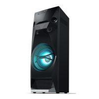
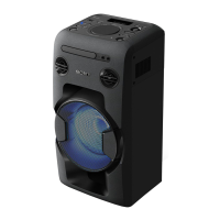
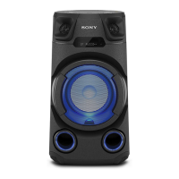
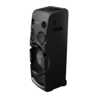
HCD-SH2000
64
Pin No. Pin Name I/O Description
69 to 74 RA9 to RA4 O Address signal output to the SD-RAM
75 RWE# O Write enable signal output to the SD-RAM
76 CAS# O Column address strobe signal output to the SD-RAM
77 RAS# O Row address strobe signal output to the SD-RAM
78 BA0 O Bank address signal output to the SD-RAM
79 DVSS18 - Ground terminal
80 BA1 O Bank address signal output to the SD-RAM
81 to 83 RA10, RA0, RA1 O Address signal output to the SD-RAM
84 DVDD33 - Power supply terminal (+3.3V)
85, 86 RA2, RA3 O Address signal output to the SD-RAM
87 IFBSY I Communication initialization request signal input from the system controller
88 IFCS# O Communication initialization request acknowledge signal output to the system controller
89 RX - Not used
90 DVDD18 - Power supply terminal (+1.8V)
91 TX - Not used
92 XMAMUTE - Not used
93 SPDIF O SPDIF signal output terminal Not used
94 GPIO I Thermal shut down signal input from the coil/motor driver
95 DACVDDC - Power supply terminal (+3.3V)
96 VREF I Band gap reference voltage terminal
97 FS I Full scale adjustment terminal
98 DACVSSC - Ground terminal
99 CVBS O Composite video signal output terminal Not used
100, 101
DACVDDB,
DACVDDA
- Power supply terminal (+3.3V)
102 SY/Y/G O Component video (Y) signal output terminal Not used
103 SC/CB/B O Component video (Pb/Cb) signal output terminal Not used
104 CR/R O Component video (Pr/Cr) signal output terminal Not used
105 AADVSS - Ground terminal
106 GPIO19 I Audio data input from the A/D converter (for USB)
107 MUTE123 - Not used
108 LIMITSW - Not used
109, 110 AADVDD, APLLVDD - Power supply terminal (+3.3V)
111 APLLCAP I External capacitor connecting terminal
112, 113
ADACVSS2,
ADACVSS1
- Ground terminal
114 GPIO O Master clock signal output to the A/D converter and D/A converter
115 GPIO O Bit clock signal output to the A/D converter and D/A converter
116 GPIO O Muting signal output to the coil/motor driver (for focus/tracking coil and sled motor)
117 AVCM - Audio D/A converter reference voltage terminal
118 GPIO I Limit detection switch input terminal
119 GPIO O L/R sampling clock signal output to the A/D converter and D/A converter
120 GPIO O Audio data output to the D/A converter
121, 122
ADACVDD1,
ADACVDD2
- Power supply terminal (+3.3V)
123 AVDD18_1 - Power supply terminal (+1.8V)
124 AGND18 - Ground terminal
125, 126 RF_IP, OPOUT I AC coupled RF signal input from the optical pick-up block
127 IOPMON/OPINP I Power monitor terminal
128 SPFG/OPINN I Spindle motor hall sensor input from the motor driver