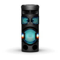
HCD-SH2000
63
DMB21 BOARD (2/3) IC101 CXD9968R (LE)
Pin No. Pin Name I/O Description
1 RF_A I RF main beam (C) input from the optical pick-up block
2 RF_B I RF main beam (B) input from the optical pick-up block
3 RF_C I RF main beam (A) input from the optical pick-up block
4 RF_D I RF main beam (D) input from the optical pick-up block
5 RF_E I RF sub beam (F) input from the optical pick-up block
6 RF_F I RF sub beam (E) input from the optical pick-up block
7 AVDD18_2 - Power supply terminal (+1.8V)
8 AVDD33_1 - Power supply terminal (+3.3V)
9 XTALI I System clock input terminal (27 MHz)
10 XTALO O System clock output terminal (27 MHz)
11 AGND33 - Ground terminal
12 V2O O Reference voltage (+2V) output to the optical pick-up block
13 V14/VREFO O Reference voltage (+1.4V) output terminal
14 REXT I Current reference input terminal Fixed at “L” in this set
15, 16 MDI1, MDI2 I Laser power monitor input from the optical pick-up block
17, 18 LDO1, LDO2 O Laser diode drive signal output to the optical pick-up block
19 AVDD33_2 - Power supply terminal (+3.3V)
20 DMO O Spindle motor control signal output to the motor driver
21 FMO O Sled motor control signal output to the motor driver
22 MUTE4 O Muting signal output to the coil/motor driver (for spindle motor)
23 MSW O CD/DVD selection signal output terminal “L”: CD, “H”: DVD
24 TRO O Tracking coil control signal output to the coil driver
25 FOO O Focus coil control signal output to the coil driver
26 EEWP - Not used
27, 28 USB_DP, USB_DM I/O Two-way audio serial data with the USB controller
29 VDD33_USB - Power supply terminal (+3.3V)
30 VSS33_USB - Ground terminal
31 PAD_VRT I/O USB generating reference current terminal
32 VDD18_USB - Power supply terminal (+1.8V)
33 SCL O Serial clock signal output terminal Not used
34 SDA I/O Two-way serial data bus terminal Not used
35 IFSDI I Serial data input from the system controller
36 FS_CS# O Chip select signal output to the fl ash ROM
37 SF_DO O Serial data output to the fl ash ROM
38 SF_DI I Serial data input from the fl ash ROM
39 SF_CK O Serial clock signal output to the fl ash ROM
40 IFSCK O Serial data transfer clock signal output to the system controller
41 IFSOD O Serial data output to the system controller
42 ICE I ICE mode enable setting terminal Not used
43 PRST# I Reset signal input from the system controller “L”: reset
44 IR I IR control signal input terminal Not used
45 to 49 RD0 to RD4 I/O Two-way data bus with the SD-RAM
50 DVDD33 - Power supply terminal (+3.3V)
51 to 53 RD5 to RD7 I/O Two-way data bus with the SD-RAM
54 DVDD18 - Power supply terminal (+1.8V)
55 DQM0 O Data mask signal output to the SD-RAM
56 to 59 RD15 to RD 12 I/O Two-way data bus with the SD-RAM
60 DVSS33 - Ground terminal
61 to 64 RD11 to RD8 I/O Two-way data bus with the SD-RAM
65 DQM1 O Data mask signal output to the SD-RAM
66 RCLK O Clock signal output to the SD-RAM
67 RA11 O Address signal output to the SD-RAM
68 DVDD33 - Power supply terminal (+3.3V)