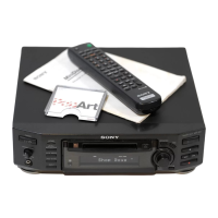
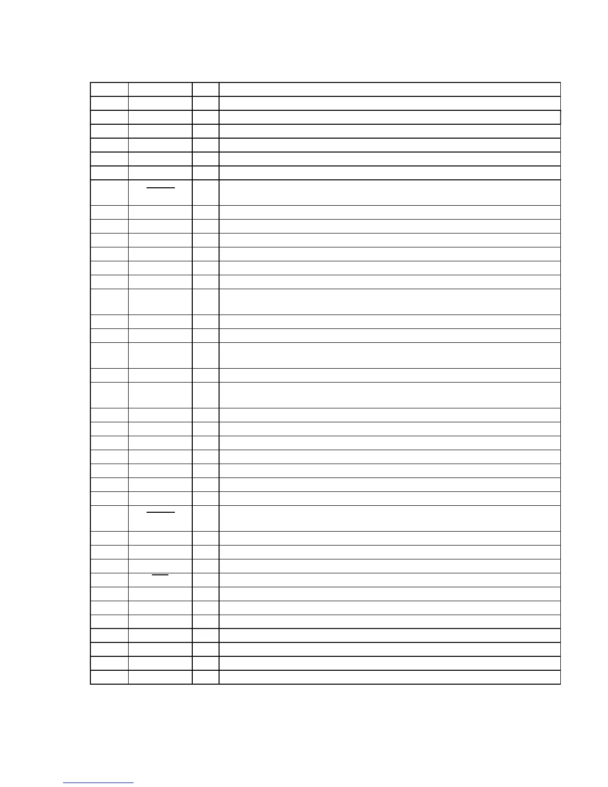
67
• MAIN BOARD IC501 M30625MGA-A50GP (CD MECHANISM CONTROL)
Pin No. Pin Name I/O Description
1NCO
Not used (open)
2 LEVEL R O
R-ch level output to the system controller (IC601)
3 LEVEL L O
L-ch level output to the system controller (IC601)
4, 5 NC O
Not used (open)
6 CNVSS —
Ground terminal
7, 8 NC O
Not used (open)
9 RESET I
System reset signal input from the reset signal generator (IC906) “L”: reset
For several hundreds msec. after the power supply rises, “L” is input, then it changes to “H”
10 XOUT O
Main system clock output terminal (10 MHz)
11 VSS —
Ground terminal
12 XIN I
Main system clock input terminal (10 MHz)
13 VCC —
Power supply terminal (+5V)
14
NMI
I
Non-maskable interrupt input terminal Fixed at “H” in this set
15 NC O
Not used (open)
16 SCOR
I
Subcode sync (S0+S1) detection signal input from the CXD2585Q (IC101) on the CD block
“H”: active
17 LPH
O Laser power control signal output to the CXD2585Q (IC101) on the CD block “H” active
18 XSEL O
Operation mode select signal output to the CXD2585Q (IC101) on the CD block “H” active
19 AMUTE O
Analog muting on/off control signal output to the CXD2585Q (IC101) on the CD block
“H”: muting on
20, 21 NC O
Not used (open)
22 I2CCLK I/O
Communication data reading clock signal input or transfer clock signal output with the system
controller (IC601)
23 I2CDATA I/O
Communication data bus with the system controller (IC601)
24 TXD1 O
Not used (open)
25 RXD1 O
Not used (open)
26 CLK1 O
Not used (open)
27 RTS1 O
Not used (open)
28 NC O
Not used (open)
29
SUBQ
I
Subcode Q data input from the CXD2585Q (IC101) on the CD block
30
SQCLK
O
Subcode Q data reading clock signal output to the CXD2585Q (IC101) on the CD block
“L”: active
31 to 33 NC O
Not used (open)
34 SPDL MUTE O
Spindle motor muting control signal outputto the spindle motor drive (IC191) on the CD block
35
DATA
O
Serial data output to the CXD2585Q (IC101) on the CD block
36 CLK O
Serial data transfer clock signal output to the CXD2585Q (IC101) on the CD block “L” active
37 XLT O
Serial data latch pulse output to the CXD2585Q (IC101) on the CD block “L” active
38
SENSE I Internal status detection monitor input from the CXD2585Q (IC101) on the CD block
39
LDON O Laser on/off control signal output to the CXA2568M (IC131) “H”: laser on
40
1/4 SW O Disc speed selection signal output to the BU4053BCFV (IC182) on the CD block
41
8/12 SW O Disc size selection signal output to the BU4053BCFV (IC182) on the CD block
42
BDSW1 O BD selection signal output Not used (open)
43
BDSW2 O BD selection signal output Not used (open)
 Loading...