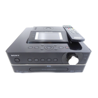
NAS-E35HD/SS-CE35HD
65
Pin No. Pin Name I/O Description
63, 64 EM_D (10), EM_D (9) I/O Two-way data bus with the SDRAM, fl ash memory and USB interface
65 CVDD - Power supply terminal (+1.2V)
66 EM_D (8) I/O Two-way data bus with the SDRAM, fl ash memory and USB interface
67 EM_WE_DQM (1) O Write enable signal output to the SDRAM
68 DVDD - Power supply terminal (+3.3V)
69 VSS - Ground terminal
70 EM_CLK O Clock signal output to the SDRAM
71 EM_CKE O Clock enable signal output to the SDRAM
72 VSS - Ground terminal
73 DVDD - Power supply terminal (+3.3V)
74 to 76
EM_A (11_12),
EM_A (9_10), EM_A (8_9)
O Address signal output to the SDRAM and fl ash memory
77 CVDD - Power supply terminal (+1.2V)
78 VSS - Ground terminal
79 EM_A (7_8) O Address signal output to the SDRAM and fl ash memory
80 EM_A (6_7) O Address signal output to the SDRAM, fl ash memory and USB interface
81 DVDD - Power supply terminal (+3.3V)
82 VSS - Ground terminal
83, 84
EM_A (5_6),
EM_A (4_5)
O Address signal output to the SDRAM, fl ash memory and USB interface
85 CVDD - Power supply terminal (+1.2V)
86 EM_A (3_4) O Address signal output to the SDRAM, fl ash memory and USB interface
87 VSS - Ground terminal
88, 89
EM_A (2_3),
EM_A (1_2)
O Address signal output to the SDRAM, fl ash memory and USB interface
90 CVDD - Power supply terminal (+1.2V)
91 EM_A (0_1) O Address signal output to the SDRAM, fl ash memory and USB interface
92 DVDD - Power supply terminal (+3.3V)
93 EM_A (10_11) O Address signal output to the SDRAM and fl ash memory
94 EM_BA (1)/EM_A (_0) O
Bank address signal output to the SDRAM,
and address signal output to the fl ash memory and USB interface
95 VSS - Ground terminal
96 EM_BA (0) O Bank address signal output to the SDRAM
97 EM_CS (0) O Chip select signal output to the SDRAM
98 EM_RAS O Row address strobe signal output to the SDRAM
99 VSS - Ground terminal
100 EM_CS (2) O Chip select signal output to the memory decoder
101 CVDD - Power supply terminal (+1.2V)
102 EM_RW - Not used
103 DVDD - Power supply terminal (+3.3V)
104 EM_OE O Output enable signal output to the fl ash memory and USB interface
105 B O Address decode signal output to the memory decoder
106 VSS - Ground terminal
107 A O Address decode signal output to the memory decoder
108 I2CO_SCL/BOOT I/O Two-way I2C serial clock signal bus with the system controller
109 VSS - Ground terminal
110 GPIO/BOOT - Not used
111 I2CO_SDA/BOOT I/O Two-way I2C serial data bus with the system controller
112 DVDD - Power supply terminal (+3.3V)
113 SDTI I Audio serial data input from the A/D converter and D/A converter
114 VSS - Ground terminal
115 SDTO_O O Audio serial data output to the A/D converter and D/A converter
116 BD_CLK O Serial data transfer clock signal output to the digital servo
117 BD_SENS I Internal status (SENSE) input from the digital servo
118 VSS - Ground terminal
119 BD_GAIN-SW O Gain switch signal output to the motor/coil driver
120 BD_XLAT O Serial data latch pulse output to the digital servo
121 BD_DATA O Serial data output to the digital servo
122 BD_SCOR I Sub-code sync (S0+S1) detection signal input from the digital servo
123 CVDD - Power supply terminal (+1.2V)