– 29 – – 30 – – 31 –
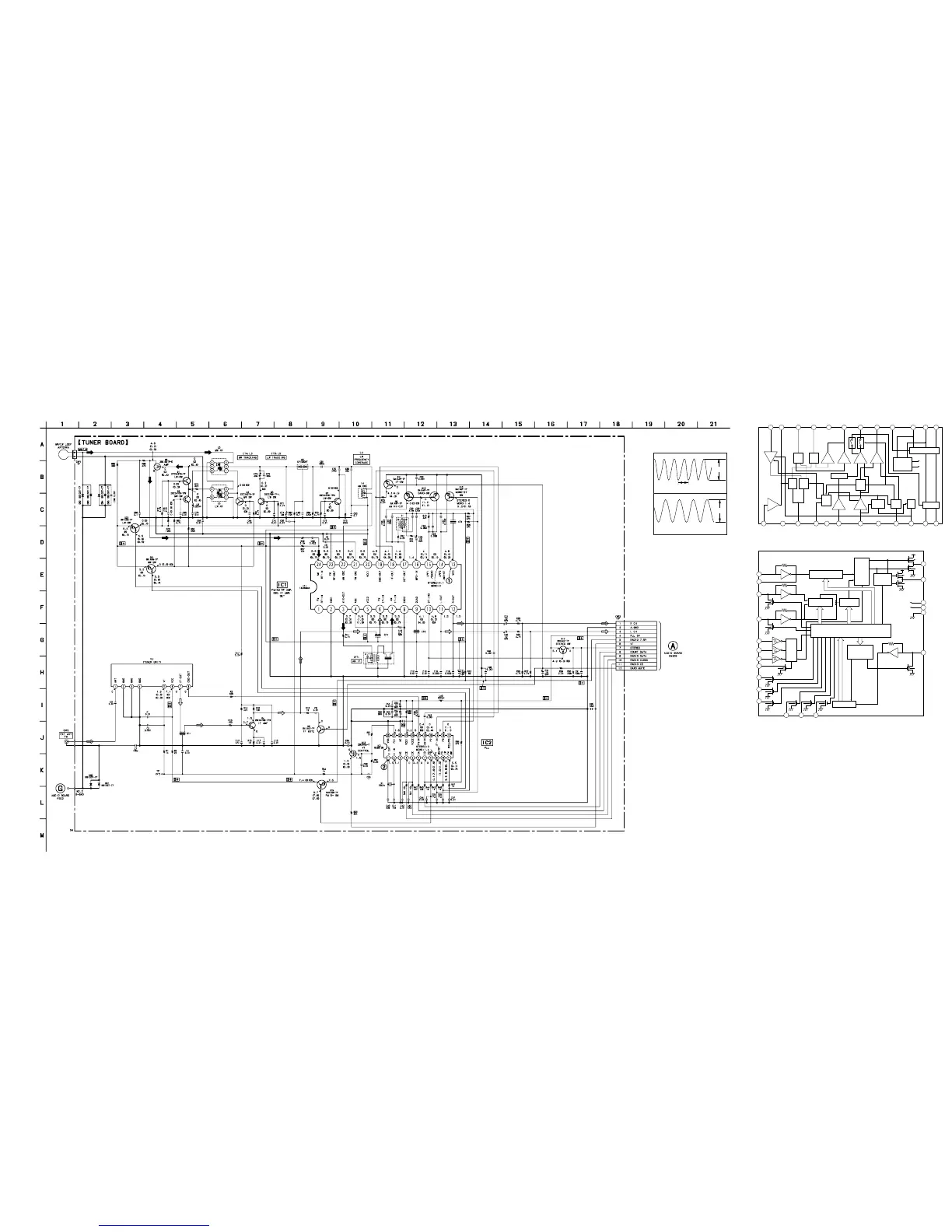
6-7. SCHEMATIC DIAGRAM — TUNER SECTION —
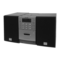
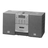
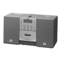
PMC-D307L
• IC Block Diagrams
IC1 TA2008AN
IC2 BU2615S
18 1314192021
10 11 1298765431 2
222324
AM
RF
FM
RF
BUFFBUFF
IF
BUFF
AF
BUFF
AM
IF
FM
IF
FM
OSC
AM
MIX
AM
DET
AGC
FM
MIX
AM
OSC
17 16
1/8DIV
LEVEL
DET
FM
DET
ST
DET
MUTE
FM MPX
15
AM/FM
ST/MONO
SW
2
19
11
18
17
20
13
1
16
15
3
4
5
6
7
PRESCALER MAIN COUNT
REFERENCE DIVIDER
I/O
CTL
8
14
SHIFT REGISTER LATCH
PHASE
DET
BUFFER
IF COUNT
CTL
20BIT COUNT
12109
ULLOCK
P5
PD1
PD2/P5
VDD1
VDD2
VSS
IF IN
P3
P4
P6
P2
P1
P0
CD
DA
CK
CE
AMIN
FMIN
XOUT
XIN
1.4Vp-p
2.2µs
• Waveforms
1
2
IC1
!£
(VCO)
IC2
1
(X OUT)
1.4Vp-p
75kHz
Note:
• All capacitors are in µF unless otherwise noted. pF: µµF
50 WV or less are not indicated except for electrolytics
and tantalums.
• All resistors are in Ω and
1
/
4
W or less unless otherwise
specified.
•
¢
: internal component.
• C : panel designation.
• U : B+ Line.
• H : adjustment for repair.
• Voltage and waveforms are dc with respect to ground
under no-signal (detuned) conditions.
no mark : FM
( ) : MW
<< >> : LW
• Voltages are taken with a VOM (Input impedance 10 MΩ).
Voltage variations may be noted due to normal produc-
tion tolerances.
• Waveforms are taken with a oscilloscope.
Voltage variations may be noted due to normal produc-
tion tolerances.
• Circled numbers refer to waveforms.
• Signal path.
F : FM
f : MW/LW
 Loading...