– 41 – – 42 – – 43 –
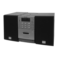
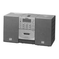
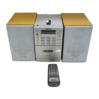
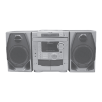
PMC-D307L
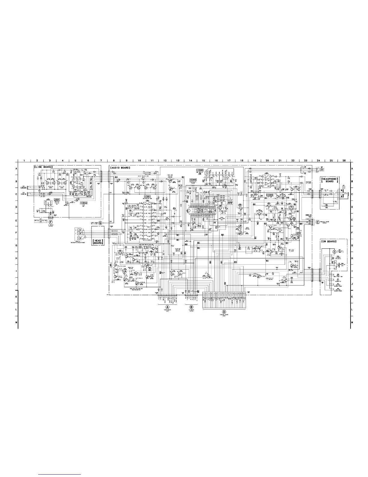
6-11. SCHEMATIC DIAGRAM — MAIN SECTION — • Refer to page 57 for IC Block Diagrams.
Note:
• All capacitors are in µF unless otherwise noted. pF: µµF
50 WV or less are not indicated except for electrolytics
and tantalums.
• All resistors are in Ω and
1
/
4
W or less unless otherwise
specified.
• C : panel designation.
• U : B+ Line.
• Voltages are dc with respect to ground under no-signal
(detuned) conditions.
no mark : FM
( ) : PB
<< >> : REC
[ ] : CD
∗
: Impossible to measure
• Voltages are taken with a VOM (Input impedance 10 MΩ).
Voltage variations may be noted due to normal produc-
tion tolerances.
• Signal path.
F : FM
E : PB
a : REC
L : LINE IN
J : CD
c : digital out