53
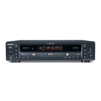
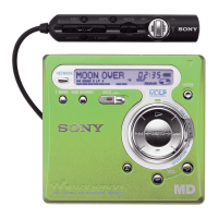
RCD-W1
Pin No. Pin Name I/O
Description
• IC801 DRIVER (uPD780232GC-LG1) (FL Board)
1 VDD1 I Power supply
2 VSS1 — Ground
3 X1 I Connected to the crystal oscillator (5MHz)
4 X2 O Connected to the crystal oscillator (5MHz)
5 IC I Internally connected. (Connect to ground)
6 RESET I System reset input
7 SCK1 I/O Serial serial clock I/O
8 SI1 I Serial data input
9 SO1 O Serial data output
10 BUSY O Not used
11 P23 O Not used
12 P22 O Not used
13 P21 O Not used
14 P20 O Not used
15 P00 I Chip select signal input
16 P01 O Not used
17 P02 I Connect to Vdd via a resistor.
18 AVSS — Ground
19 ANI3 I Connect to Vdd via a resistor.
20 ANI2 I Connect to Vdd via a resistor.
21 ANI1 I Connect to Vdd via a resistor.
22 ANI0 I Connect to Vdd via a resistor.
23 VSS0 — Ground
24 AVDD I Power supply
25 VDD0 I Power supply
26 P64 — Not used
27 P63 — Not used
28 P62 — Not used
29 P61 — Not used
30 P60 — Not used
31 P57 — Not used
32 P56 — Not used
33 P55 — Not used
34 P54 — Not used
35 P53 — Not used
36 P52 — Not used
37 P51 — Not used
38 P50 I Connect to Vdd via a resistor.
39 P47 — Not used
40 P46 — Not used
41 F37 — Not used
42 F36 — Not used
43 F35 O Fluorescent disply tube segment signal output
44 F34 O Fluorescent disply tube segment signal output
45 F33 O Fluorescent disply tube segment signal output
46 F32 O Fluorescent disply tube segment signal output
47 F31 O Fluorescent disply tube segment signal output
48 F30 O Fluorescent disply tube segment signal output
49 F29 O Fluorescent disply tube segment signal output
50 F28 O Fluorescent disply tube segment signal output