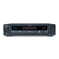
Do you have a question about the Sony RCD-W1 and is the answer not in the manual?
Detailed technical specifications for the CD player and recorder sections.
Information on similar mechanisms used in the product.
Precautions for handling pick-up, laser emission, and safety checks.
Guidelines for chip components, flex boards, and safety components.
Explanations for various error messages displayed by the unit.
Important notes and precautions for service personnel.
Procedure for removing the top case of the unit.
Steps to remove the tray door and front panel assembly.
Instructions for removing the HP, FL, and VOL boards.
Procedure for removing the back panel.
Steps to remove the audio board.
Instructions for removing the power board.
Procedure for removing the CD player and CD-R deck assemblies.
Steps to remove the BD board for Deck A.
Instructions for removing the CDP mechanism assembly for Deck A.
Procedure for removing the spindle motor and pick-up block for Deck A.
Steps to remove the BD-R board for Deck B.
Instructions for removing the CD-R mechanism assembly for Deck B.
Procedure for removing the sled mechanism assembly.
Details on adjusting the laser diode power using specific jigs.
List of required jigs and software environment for LD power adjustment.
Explanation of the parameters checked during the LD setting check.
Numerical specifications for each parameter in the LD setting check.
Explanation of VRDC, VWDC1, VWDC2, and VWDC2 Offset parameters.
Numerical ranges for parameters like read and write power.
Steps to perform the adjustment data check using the calibration menu.
Servicing notes and checks for the CD playback section.
Procedures for checking RF signal level and E-F balance using an oscilloscope.
Procedure to check the RF signal level for the CD-R section.
Checking E-F balance for the CD-R section in 1-track jump mode.
Visual representation of the location of all circuit boards within the unit.
Waveforms related to the CD-R and CD playback sections.
Waveforms related to the panel section.
Block diagram illustrating the CD-R section circuitry.
Continuation of the block diagram for the CD-R section.
Block diagram detailing the CD playback section.
Block diagram of the audio processing circuitry.
Block diagram illustrating the power supply circuitry.
Printed wiring board layout for the CD-R section (Side A).
Printed wiring board layout for the BD-R board (Side B).
Schematic diagram of the CD-R section, part 1 of 6.
Schematic diagram of the CD-R section, part 2 of 6.
Schematic diagram of the CD-R section, part 3 of 6.
Schematic diagram of the CD-R section, part 4 of 6.
Schematic diagram of the CD-R section, part 5 of 6.
Schematic diagram of the CD-R section, part 6 of 6.
Printed wiring board layout for the CDP section (Side A).
Printed wiring board layout for the BD board (Side B).
Schematic diagram of the CDP section, part 1 of 3.
Schematic diagram of the CDP section, part 2 of 3.
Schematic diagram of the CDP section, part 3 of 3.
Schematic diagram of the audio section, part 1 of 2.
Schematic diagram of the audio section, part 2 of 2.
Printed wiring board layout for the audio section (Sides A and B).
Printed wiring board layouts for the FL, VOL, and HP panels.
Schematic diagrams for the panel sections.
Printed wiring board layout for the power supply section.
Schematic diagram for the power supply section.
Detailed pin function descriptions for IC501.
Pin function description for IC701.
Continuation of pin function description for IC701.
Pin function description for IC801.
Continuation of pin function description for IC801.
Block diagram for IC201.
Block diagrams for IC306, IC501, and IC510.
Block diagram for IC401.
Block diagrams for IC301 and IC401.
Block diagram for IC201.
Block diagrams for IC101 and IC105,401.
Exploded view of the front panel components.
Exploded view of the chassis and main internal components.
Exploded view of the CD play mechanism for Deck A.
Exploded view of the CD record mechanism for Deck B.
Electrical parts list specifically for the audio section.
Continuation of the electrical parts list for the audio section.
Electrical parts list for the BD-R board.
Continuation of the electrical parts list for the BD-R board.
Continuation of the electrical parts list for BD and BD-R boards.
Continuation of the electrical parts list for BD-R and FL boards.
Continuation of the electrical parts list for BD-R and FL boards.
Continuation of the electrical parts list for BD-R and FL boards.
Continuation of the electrical parts list for BD-R and FL boards.
Continuation of the electrical parts list for BD-R and FL boards.
Electrical parts list for FL, HP, and POWER boards.
Electrical parts list for POWER and VOL boards.
Record of revisions made to the service manual.
| Type | CD Recorder |
|---|---|
| Audio Output | Analog, Digital |
| Recording Media | CD-R, CD-RW |
| Playback Formats | CD, CD-R, CD-RW |
| Weight | 4.0 kg |
| Frequency Response | 20 Hz - 20 kHz |
| Digital Input | Coaxial, Optical |
| Digital Output | Coaxial, Optical |
| Channels | 2 |
| Output Level | 2 V |