43
RCD-W3
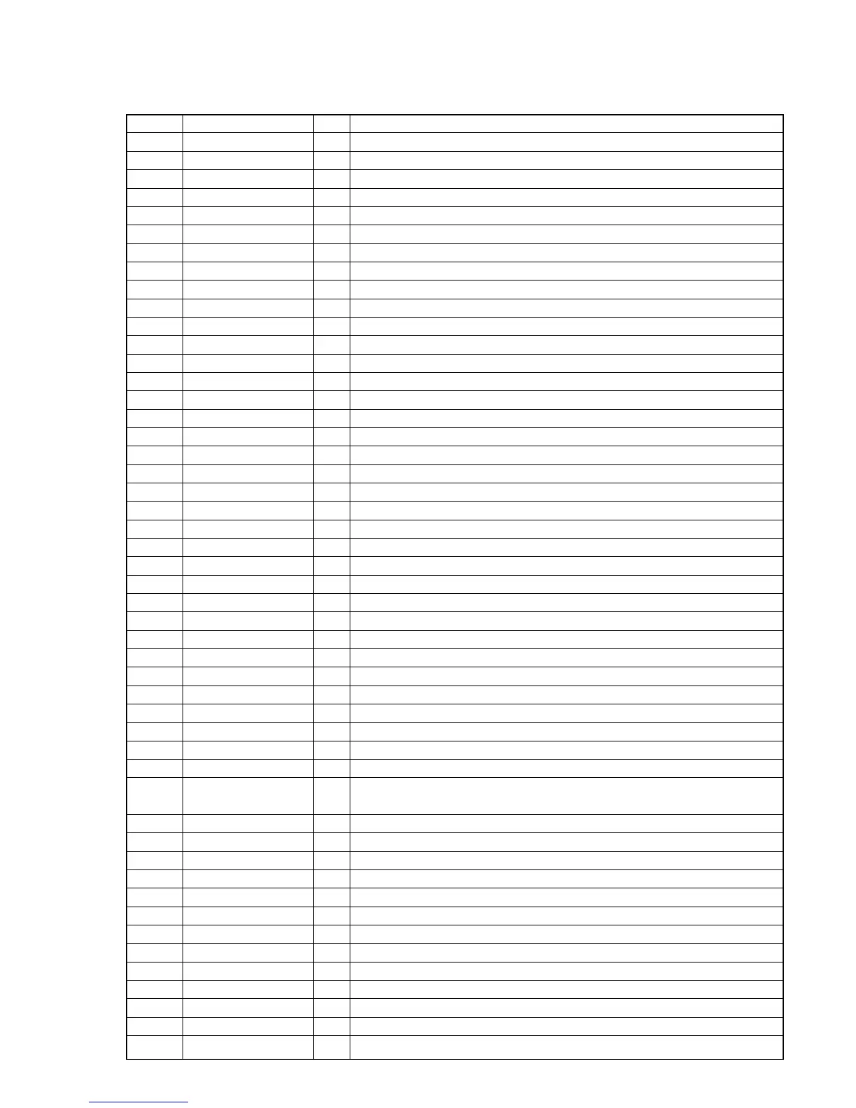
Pin No. Pin Name I/O
Description
• IC203 HD64F3062BFBL-W3CDR (SYSTEM CONTROL) (BD-R BOARD (3/6))
1 VCL — Not used (connected to ground through capacitor)
2 ATIP/EFM O ATIP/EFM signal output to CST0100C
3 /DA_RCS O Chipselect signal output to VC01S05
4 /UCS1 O Mode set signal output to OTI-9790CE
5 /UCS0 O Mode set signal output to OTI-9790CE
6 DA_RCLK O Clock output to VC01S05
7 WR/nRE O Read or write (CPLD) select signal output
8 /OAK_RST O Reset signal output for OTI-9790CE
9 DA_RDATA O Data output to VC01S05
10 FWE I Flash memory write enable
11 VSS — Ground
12 REC_TXD O Serial data output to CDP
13 BTS_TXD O Flash write data output
14 REC_RXD I Serial data input from CDP
15 BTS_RXD I Receive data from flash read
16 TRK INC I Clock input from to CDP
17 /SDINT — Not used (open)
18 SDATA_OUT O Serial data output to EEPROM
19 SCLK O Serial clock to EEPROM
20 CDR/nRW O CDR/CDRW select signal output
21 /EP_CS O EEPROM chip selector signal output
22 VSS — Ground
23 /CXA_CS O CXA3558R chip select signal output
24 /DA_CS O DAC chip select signal output
25 TP(I/O) I/O Not used (pull down)
26 TP(I/O) I/O Not used
27 to 34 UAD0 to 7 I/O Data BUS
35 VCC — Power supply
36 to 43 UA0 to 7 O Address BUS
44 VSS — Ground
45 UA8 O Address BUS
46 /OPEN_SW I OPEN switch signal input
47 /LOAD_SW I LOAD switch signal input
48 RECD1 I RECD1 signal input from CXA3558R
49 /SLD_IN_SW I SLD-IN switch signal input
50
A_DATA_ZERO
(JIG_DOWN)
I Not used (pull down)
51 SRC_INT (HOT_TX) I Serial data input from CS8420-CSR
52 SRC_DIN (HOT_RX) I Interrupt signal input from CS8420-CSR
53 XTOK I XTOK signal input from CXA3558R
54 TP (IN) I Not used
55 OPTION-1 I Not used
56 FLAGB I Servo flag input
57 VSS — Ground
58 /WAIT (URDY) I Data ready signal input from OTI-9790CE
59 AGCON O AGC on signal output to CXA3558R
60 ROPCON O ROPC related CPLD signal output
61 SDATA_IN I Serial data input from EEPROM
62 /STBY I Hardware standby signal input (connected to VCC)
63 /RESET I Reset signal input
5-18. IC PIN FUNCTION DESCRIPTION

 Loading...