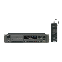
21
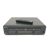
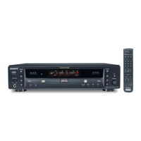
RCD-W3
SECTION 5
DIAGRAMS
• Indication of transistor
C
These are omitted
EB
Q
C
These are omitted
EB
THIS NOTE IS COMMON FOR PRINTED WIRING
BOARDS AND SCHEMATIC DIAGRAMS.
(In addition to this, the necessary note is printed
in each block.)
For schematic diagrams.
Note:
• All capacitors are in µF unless otherwise noted. pF: µµF
50 WV or less are not indicated except for electrolytics
and tantalums.
• All resistors are in Ω and
1
/
4
W or less unless otherwise
specified.
• % : indicates tolerance.
•
¢
: internal component.
• C : panel designation.
For printed wiring boards.
Note:
• : Pattern from the side which enables seeing.
(The other layers' patterns are not indicated.)
• A : B+ Line.
• B : B– Line.
• H : adjustment for repair.
• AC voltage readings in the bias oscillator with a level
meter.
• Voltages and waveforms are dc with respect to ground
under no-signal conditions.
no mark : STOP
( ) : PLAY
< > : REC (CD-R only)
• Voltages are taken with a VOM (Input impedance 10 MΩ).
Voltage variations may be noted due to normal produc-
tion tolerances.
• Waveforms are taken with a oscilloscope.
Voltage variations may be noted due to normal produc-
tion tolerances.
• Circled numbers refer to waveforms.
Note:
The components identified by
mark ! or dotted line with mark
! are critical for safety.
Replace only with part number
specified.
• Signal path.
J : CD
c : CD (digital)
I : CD REC
L : CD REC (digital)
Caution:
Pattern face side: Parts on the pattern face side seen from the
(Side B) pattern face are indicated.
Parts face side: Parts on the parts face side seen from the
(Side A) parts face are indicated.
• Abbreviation
CND : Canadian model
• Abbreviation
CND : Canadian model
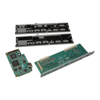
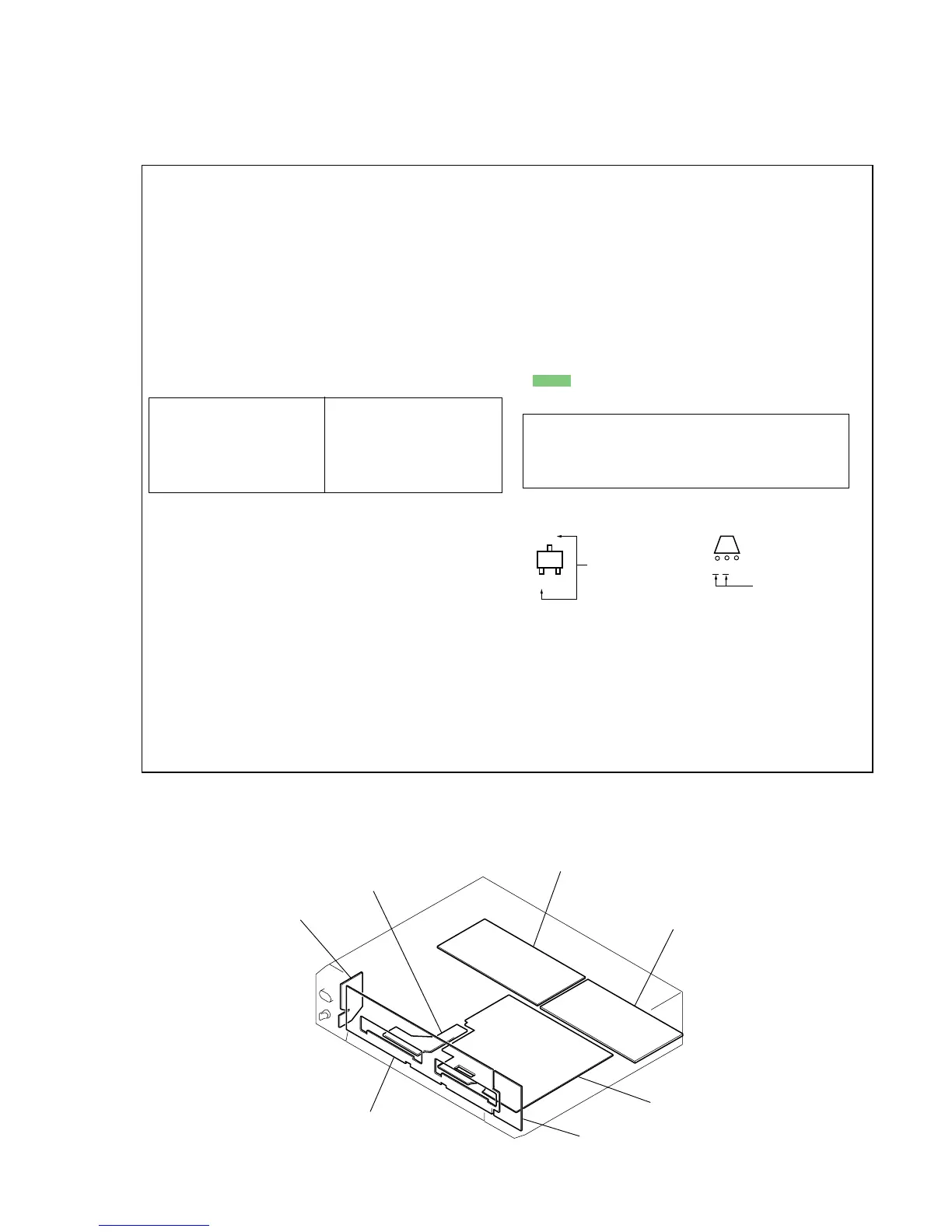
5-1. CIRCUIT BOARDS LOCATION
HP board
FL board
VOL board
BD-P board
POWER board
AUDIO
board
BD-R board
Les composants identifiés par
une marque
! sont critiques pour la sécurité.
Ne les remplacer que par une
piéce portant le numéro spécifié.
 Loading...