AN3320 Power supplies
Doc ID 18267 Rev 2 9/29
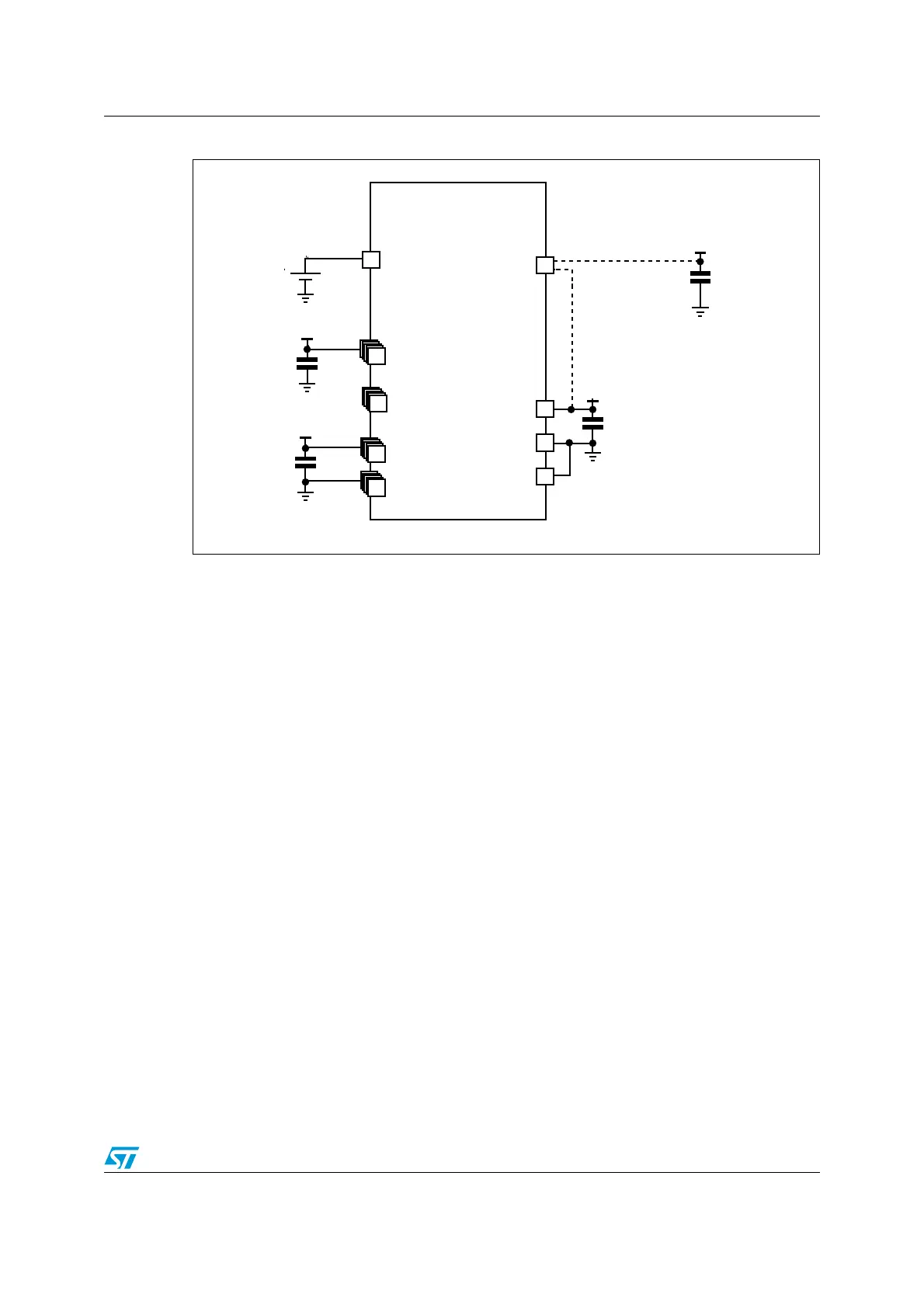
Figure 2. Power supply scheme
1. Optional. If a separate, external reference voltage is connected on V
REF+
, the two capacitors (100 nF and
1 µF) must be connected.
2. V
REF
+ is either connected to V
REF
or to V
DDA
.
3. N is the number of V
DD
and V
SS
inputs.
4. Refer to section "Voltage regulator" in STM32F20xxx/21xxx datasheet to connect REGOFF and IRROFF
pins.
1.3 Reset & power supply supervisor
1.3.1 Power on reset (POR) / power down reset (PDR)
The device has an integrated POR/PDR circuitry that allows proper operation starting from
1.8 V.
The device remains in the Reset mode as long as V
DD
is below a specified threshold,
V
POR/PDR
, without the need for an external reset circuit. For more details concerning the
power on/power down reset threshold, refer to the electrical characteristics in
STM32F20xxx/21xxx datasheets.
On WLCSP66 package if IRROFF pin is set to V
DD
(in that case REGOFF pin must not be
activated, refer to section "Voltage regulator" in STM32F20xxx/21xxx datasheet for details ),
the PDR is not functional. Then the V
DD
can lower below 1.8 V, but the external circuitry
must ensure that reset pin is activated when V
DD
/V
DDA
becomes below 1.65 V.
6
"!4
34-&XXXXXX
.§N&
6
$$
§&
N&&
N&&
NOTE
"ATTERY
6
"!4
6
2%&
6
$$!
6
33!
6
2%&n
6
$$.
6
33.
6
2%&
6
$$
!)B
6
#!0
§&
6
#!0
2%'/&&
)22/&&
 Loading...


