UM2324 Rev 4 27/43
UM2324 Hardware layout and configuration
42
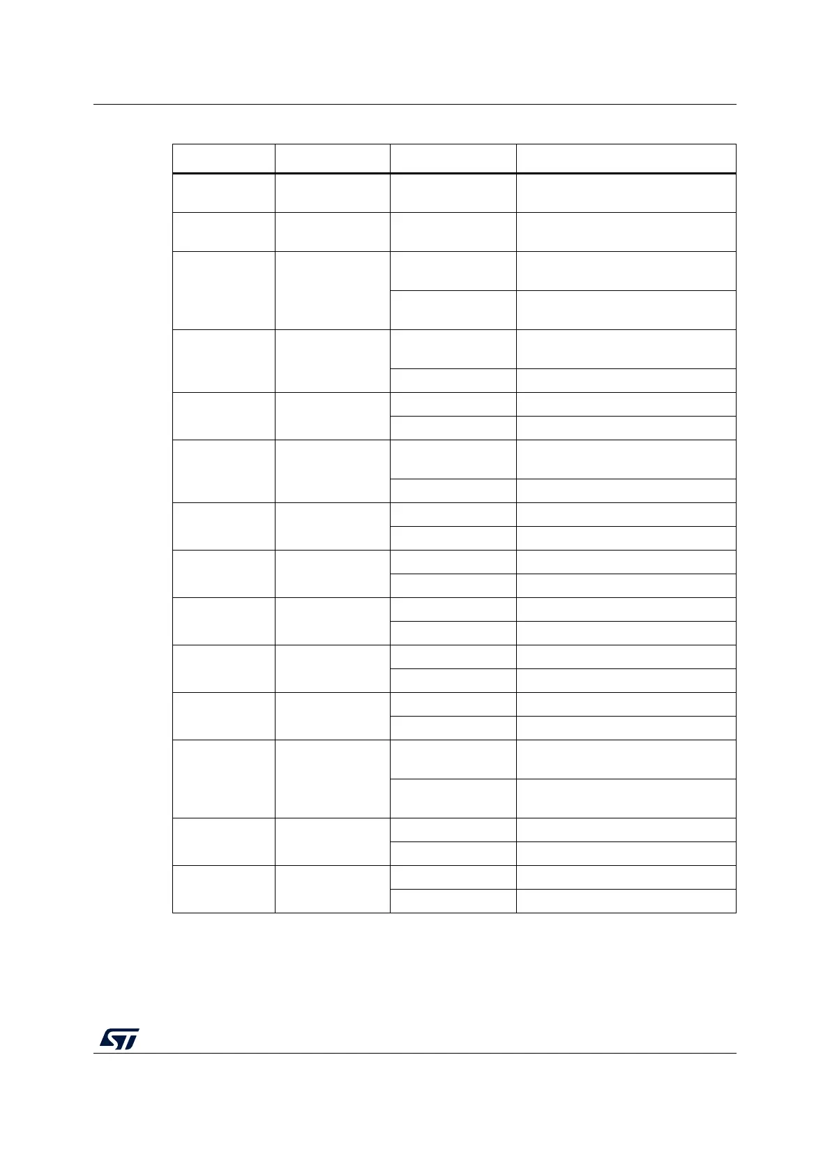
UART2 interface
(reserved)
SB16/SB18 ON
UART2 connect STLK and MCU on
board
UART2 interface
(reserved)
SB16/SB18 OFF UART2 is used as GPIOs
Allowed current
through CN2
Setting
SB15
ON
Allowed current through CN2: 100 mA
max
OFF
Allowed current through CN2: 300 mA
max
MCO SB17
ON
MCO from STLK provide 8 MHz CLK
to MCU
OFF MCO from STLK floating
3.3 V LDO
output
SB1
ON U6 LDO output provides 3.3 V
OFF U6 LDO output does not provide 3.3 V
Power
(reserved)
SB29/SB30
ON
PD8 is used as VDD, PD9 is used as
GND
OFF PD8 and PD9 is used as GPIOs
VBAT SB26
ON VDD provides power to VBAT
OFF VDD does not provide power to VBAT
AVDD SB28
ON VDD provides power to AVDD
OFF VDD does not provide power to AVDD
AGND SB31
ON AGND connects to GND
OFF AGND does not connect to GND
HSE CLK
selection
SB25/SB27
ON(R33/R34 OFF) PF0/PF1 works as GPIOs
OFF PF0/PF1 works as HSE pins
LSE CLK
selection
SB23/SB24
ON(R31/R32 OFF) PC14/PC15 works as GPIOs
OFF PC14/PC15 works as LSE pins
ADC/IIC SB2/SB3/SB4/SB5
SB3/SB4 ON,
SB2/SB5 OFF
CN8 PIN5/6 works as ADC
SB3/SB4 OFF,
SB2/SB5 ON
CN8 PIN5/6 works as IIC
User LED SB22
ON PA5 controls LD4
OFF LD4 is isolated
AVDD SB21
ON AVDD connects to CN5 PIN8
OFF AVDD disconnects to CN5 PIN8
1. Default jumper state is shown in bold.
Table 10. Solder bridge configurations and settings (continued)
Definition Bridge State
(1)
Comment
 Loading...