RM0440 Rev 4 421/2126
RM0440 Direct memory access controller (DMA)
423
12.6.6 DMA channel x memory address register (DMA_CMARx)
Address offset: 0x14 + 0x14 * (x - 1), (x = 1 to 8)
Reset value: 0x0000 0000
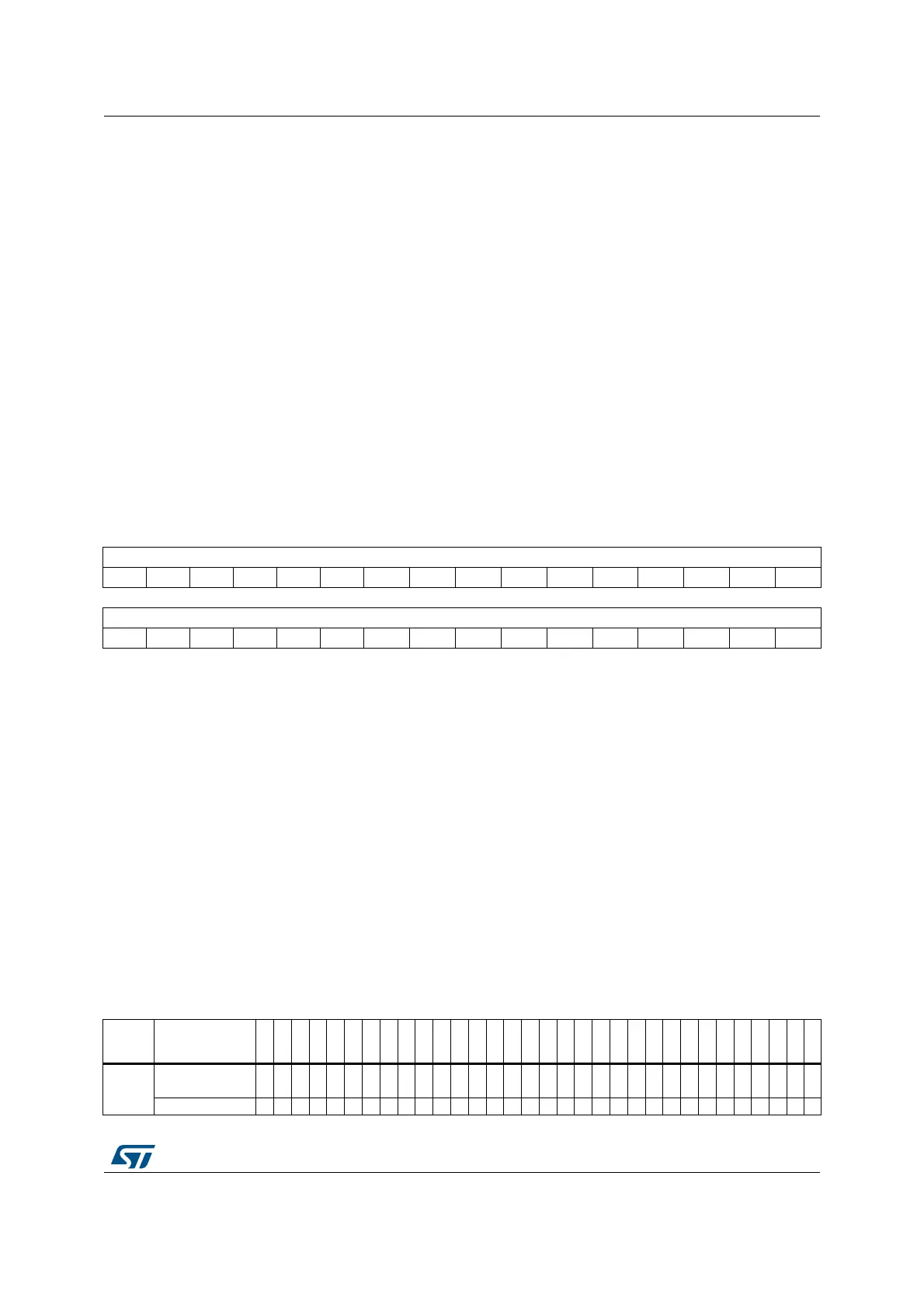
12.6.7 DMA register map
The table below gives the DMA register map and reset values.
Bits 31:0 PA[31:0]: peripheral address
It contains the base address of the peripheral data register from/to which the data will be
read/written.
When PSIZE[1:0] = 01 (16 bits), bit 0 of PA[31:0] is ignored. Access is automatically aligned
to a half-word address.
When PSIZE = 10 (32 bits), bits 1 and 0 of PA[31:0] are ignored. Access is automatically
aligned to a word address.
In memory-to-memory mode, this register identifies the memory destination address if
DIR = 1 and the memory source address if DIR = 0.
In peripheral-to-peripheral mode, this register identifies the peripheral destination address
DIR = 1 and the peripheral source address if DIR = 0.
Note: this register is set and cleared by software.
It must not be written when the channel is enabled (EN = 1).
It is not read-only when the channel is enabled (EN = 1).
31 30 29 28 27 26 25 24 23 22 21 20 19 18 17 16
MA[31:16]
rw rw rw rw rw rw rw rw rw rw rw rw rw rw rw rw
1514131211109876543210
MA[15:0]
rw rw rw rw rw rw rw rw rw rw rw rw rw rw rw rw
Bits 31:0 MA[31:0]: peripheral address
It contains the base address of the memory from/to which the data will be read/written.
When MSIZE[1:0] = 01 (16 bits), bit 0 of MA[31:0] is ignored. Access is automatically aligned
to a half-word address.
When MSIZE = 10 (32 bits), bits 1 and 0 of MA[31:0] are ignored. Access is automatically
aligned to a word address.
In memory-to-memory mode, this register identifies the memory source address if DIR = 1
and the memory destination address if DIR = 0.
In peripheral-to-peripheral mode, this register identifies the peripheral source address
DIR = 1 and the peripheral destination address if DIR = 0.
Note: this register is set and cleared by software.
It must not be written when the channel is enabled (EN = 1).
It is not read-only when the channel is enabled (EN = 1).
Table 89. DMA register map and reset values
Offset Register
31
30
29
28
27
26
25
24
23
22
21
20
19
18
17
16
15
14
13
12
11
10
9
8
7
6
5
4
3
2
1
0
0x000
DMA_ISR
TEIF8
HTIF8
TCIF8
GIF8
TEIF7
HTIF7
TCIF7
GIF7
TEIF6
HTIF6
TCIF6
GIF6
TEIF5
HTIF5
TCIF5
GIF5
TEIF4
HTIF4
TCIF4
GIF4
TEIF3
HTIF3
TCIF3
GIF3
TEIF2
HTIF2
TCIF2
GIF2
TEIF1
HTIF1
TCIF1
GIF1
Reset value 00000000000000000000000000000000